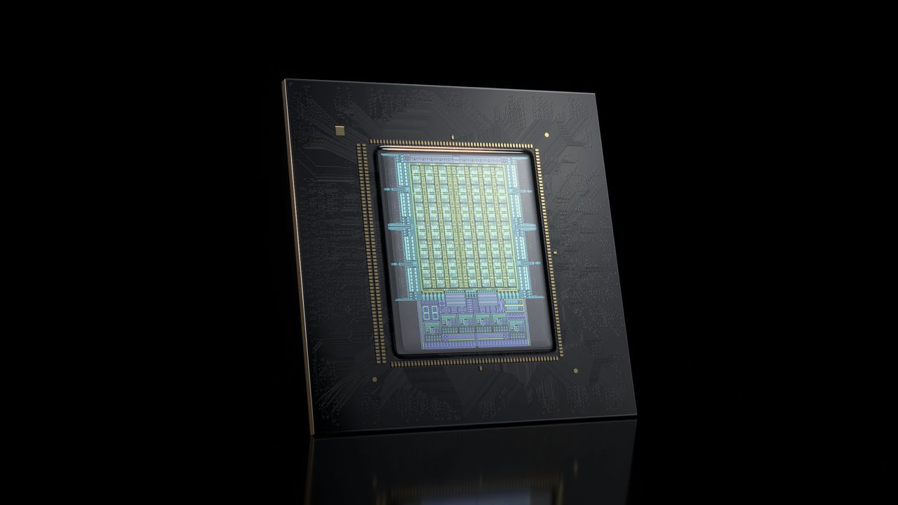
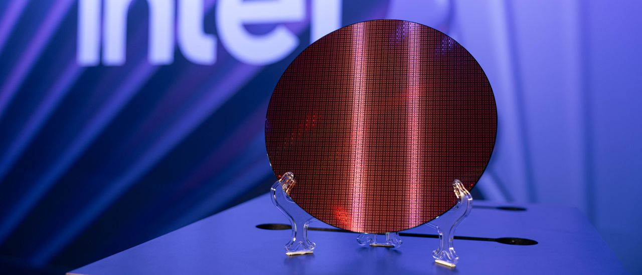
Intel won't launch a Nova Lake-S SKU with 12 Xe3P graphics cores, according to tipster Jaykihn, who originally flagged a beefed-up APU design with the Nova Lake architecture. The original SKU was said to come with 4 P-cores, 8 E-cores, and 4 LPE-cores, along with the 12 Xe3P cores, presumably offering an inexpensive onramp to a gaming desktop without a discrete GPU. Now, the leaker says that design is cancelled, and Intel intends to pick it back up with Razor Lake, the generation that will follow Nova Lake.
Nova Lake -S 12Xe has been changed to Razor Lake -S 12XeSeptember 14, 2026
Originally, Intel's 12 Xe3P Nova Lake SKU was said to require 65W of dedicated power to drive the iGPU, necessitating the use of two VCCGT phases on the motherboard for integrated graphics. Intel's Arc B390 GPU, which is the 12 Xe3-core model available in Panther Lake and Arc G-series processors, has a thermal design that can sustain up to 80W. However, it's currently being used in Panther Lake machines and handhelds like MSI Claw 8 EX AI+ that have lower power targets.
The Xe3P architecture is slotted for use in Intel's Crescent Island AI accelerator, but it hasn't been announced for any other products yet. Xe3P supports a wide deployment of Xe cores (up to 32), a deeper XMX engine with support for low-precision data types like FP8 and FP4, an increased 512KB L1 cache per Xe core, and a new unified L2 cache (32MB on Crescent Island).
Even by desktop APU standards, an 80W iGPU is a beefy accelerator to have on the same package. In addition, Intel's Nova Lake stack is said to extend up to a 175W TDP with the rumored top-end 52-core SKU, meaning the full 12 Xe3P iGPU would likely only be possible lower down the stack (and maybe only in the 4 + 8 + 4 + 12 Xe design originally suggested).
Earlier in the year, rumors suggested Intel was working on a mobile APU to counter AMD's Strix/Gorgon Halo products, featuring a large pool of unified memory and a large iGPU, dubbed Nova Lake AX. Now, the rumor mill suggests Intel will recycle the Nova Lake CPU cores for Razor Lake AX on mobile while pushing a larger iGPU.
Nova Lake-S rumored specifications
SKU*
Core Config (P+E+LPE)*
bLLC*
TDP (Unlocked/Locked)*
52 Cores (dual-tile)
(8+16)+(8+16)+4
288MB
175W
44 Cores (dual-tile)
(8+12)+(8+12)+4
264MB
175W
28 Cores
8+16+4
144MB
125W
28 Cores
8+16+4
-
125W / 65W
24 Cores
8+12+4
132MB
125W
24 Cores
8+12+4
-
125W / 65W
22 Cores
6+12+4
108MB
125W / 65W
22 Cores
6+12+4
-
125W / 65W
16 Cores
4+8+4
-
65W / 35W
12 Cores
4+4+4
-
65W / 35W
8 Cores
4+0+4
-
65W / 35W
6 Cores
2+0+4
-
65W / 35W
*Specs rumored, unconfirmed by Intel
Intel has told us that Nova Lake is one of the most important desktop CPU launches for the company ever, following on the heels of the mediocre Arrow Lake rollout. Perhaps the biggest addition to the lineup is rumored to be bLLC, or big last-level cache, which is said to show up on select SKUs to counter AMD's X3D assault among the best CPUs for gaming. The company has yet to confirm that bLLC is even possible with its current packaging capabilities, though enthusiast channel VP Robert Hallock hinted to Tom's Hardware that Intel has plans to address X3D in the next generation.
The main stack is rumored to climb up to 28 cores, with two additional dual-tile SKUs that can go as high as 52 cores. The dual-tile models look like a bid for HEDT, perhaps competing with AMD's Threadripper CPUs, though it's not clear how Intel will position its dual-tile models yet.
Alongside Nova Lake, Intel will introduce the new LGA1954 socket, along with the flagship Z990 chipset. We've already seen multiple Z990 motherboards in the flesh, suggesting Intel is preparing for a Nova Lake release in short order.
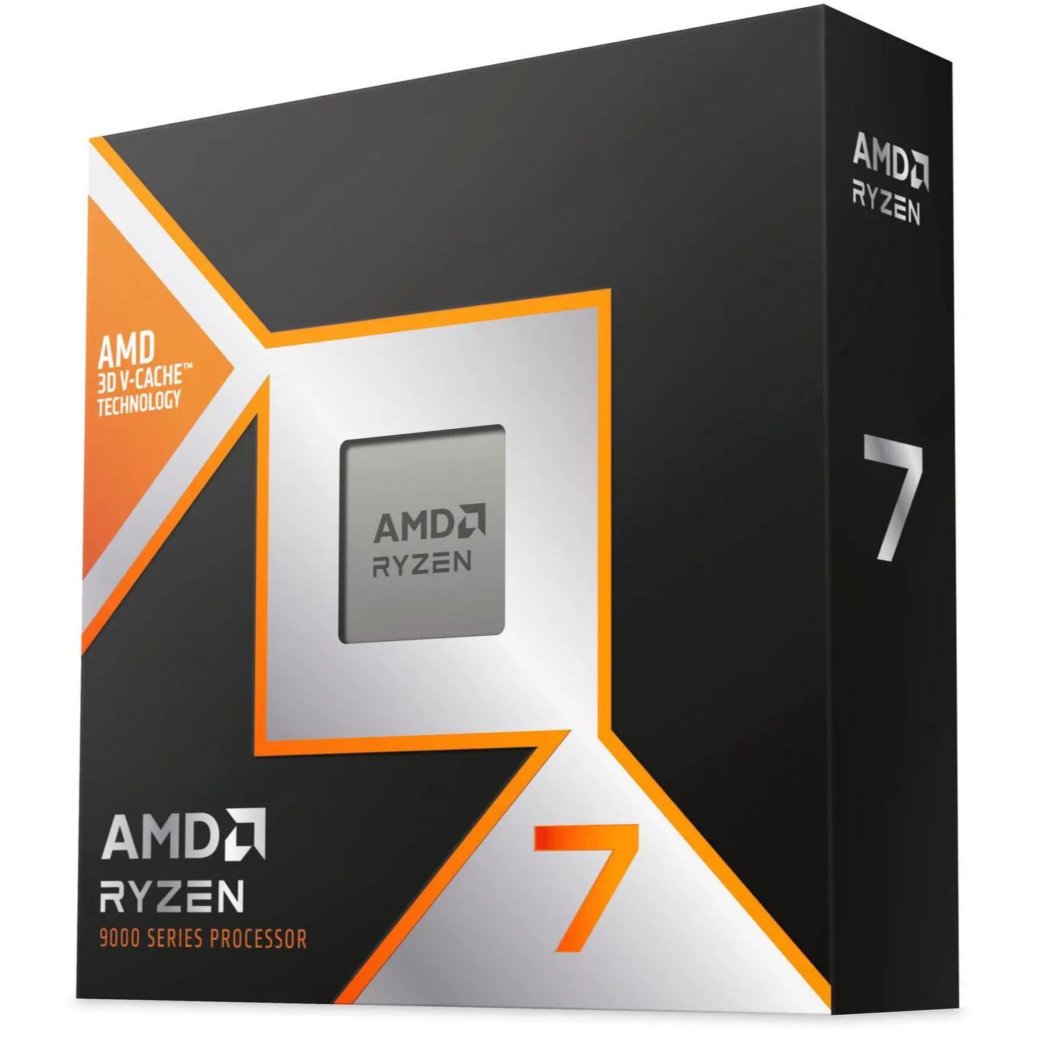
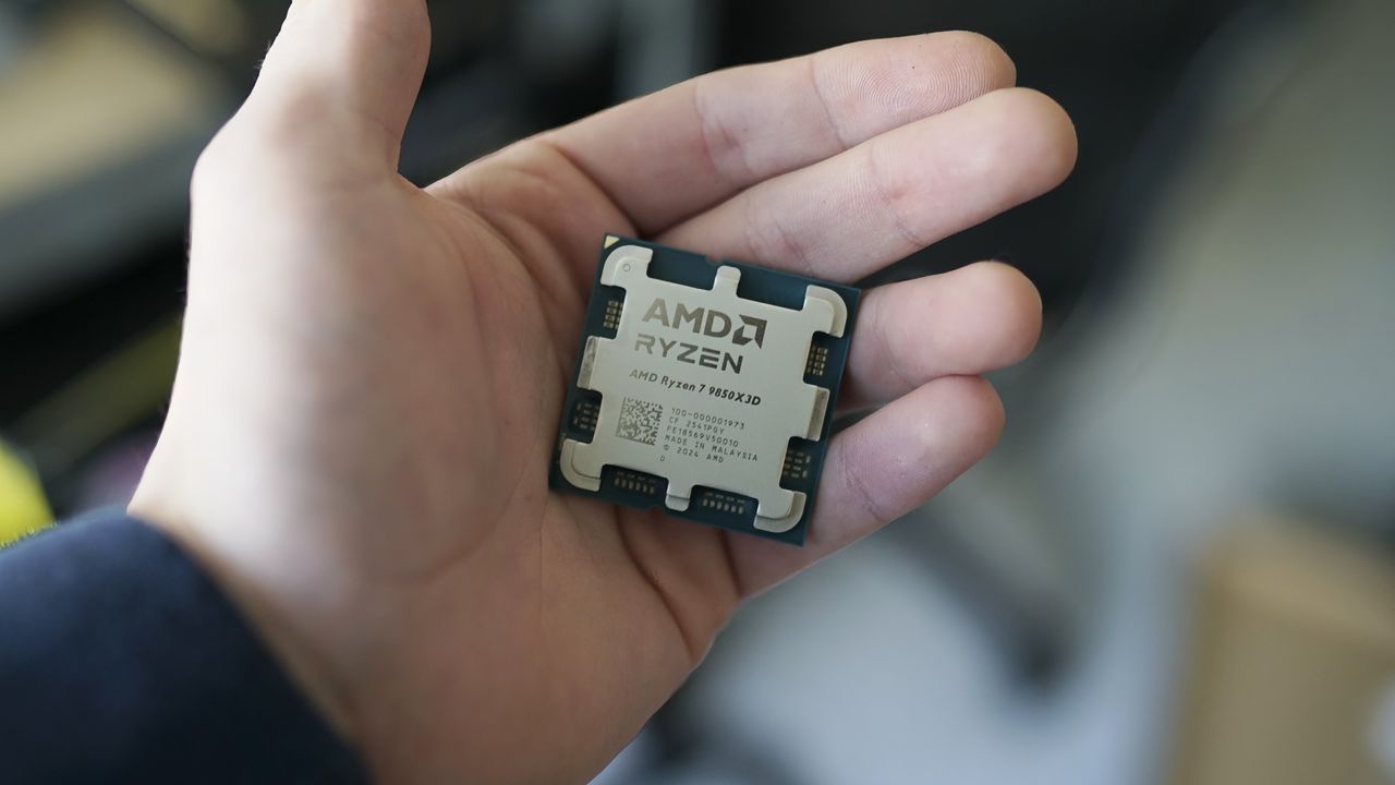
For those seeking the highest performance for gaming, AMD’s Ryzen 7 9850X3D is currently the best CPU money can buy. If you’re planning to upgrade or build a new PC, now might be a good time to pick one up, as Newegg is selling the 9850X3D for $484, around $15 less than its launch price. The deal also includes a 240mm Cooler Master AIO liquid cooler, valued at $79.99, along with a copy of Onimusha: Way of the Sword worth $69.99, both included as free gifts.
Announced at CES 2026, the Ryzen 7 9850X3D is essentially a higher-binned version of the Ryzen 7 9800X3D. It retains the same 8-core, 16-thread configuration and 4.2 GHz base clock as its predecessor, but gets a higher 5.6 GHz boost clock. The chip comes with the same 104MB of total cache, including 96MB of 3D V-Cache, which is the key ingredient behind its strong gaming performance. It also shares the same 120W default TDP and uses the AM5 platform with DDR5 memory support, making it compatible with a wide range of existing 800- and 600-series AMD motherboards.
Built on AMD’s Zen 5 architecture, the Ryzen 7 9850X3D combines 8 cores and 16 threads with a 5.6GHz boost clock and 96MB of 3D V-Cache.View Deal
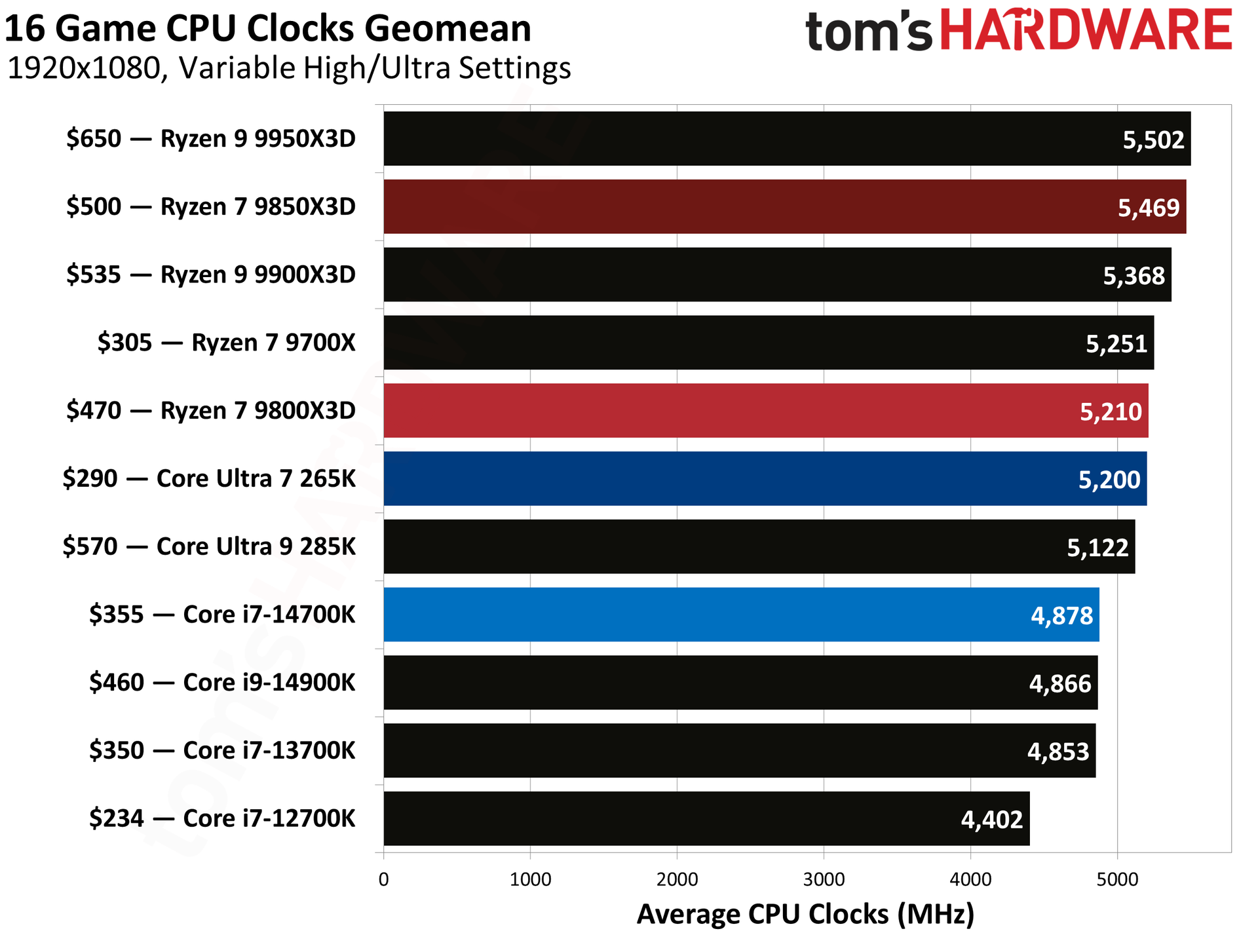
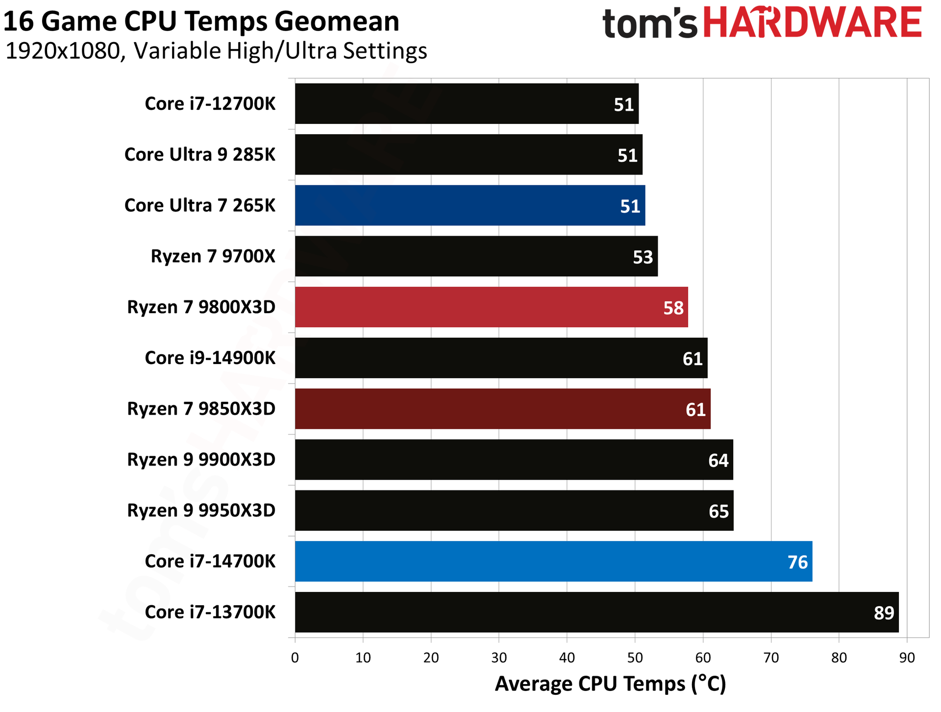
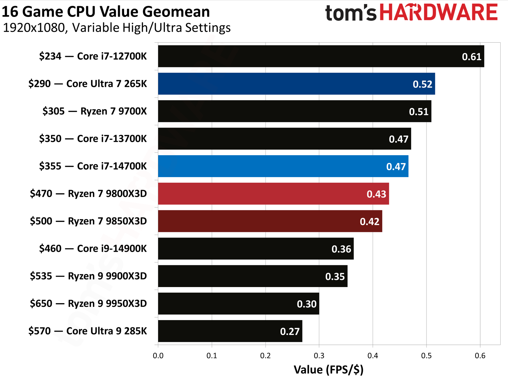
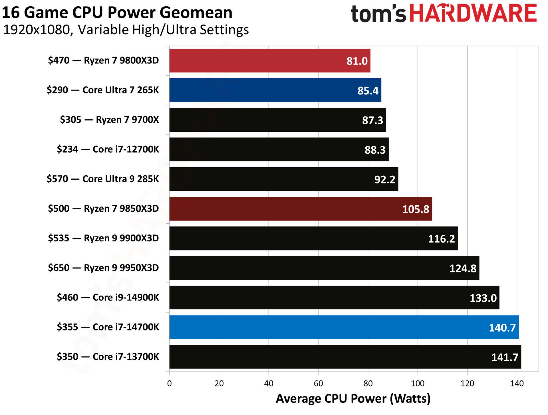
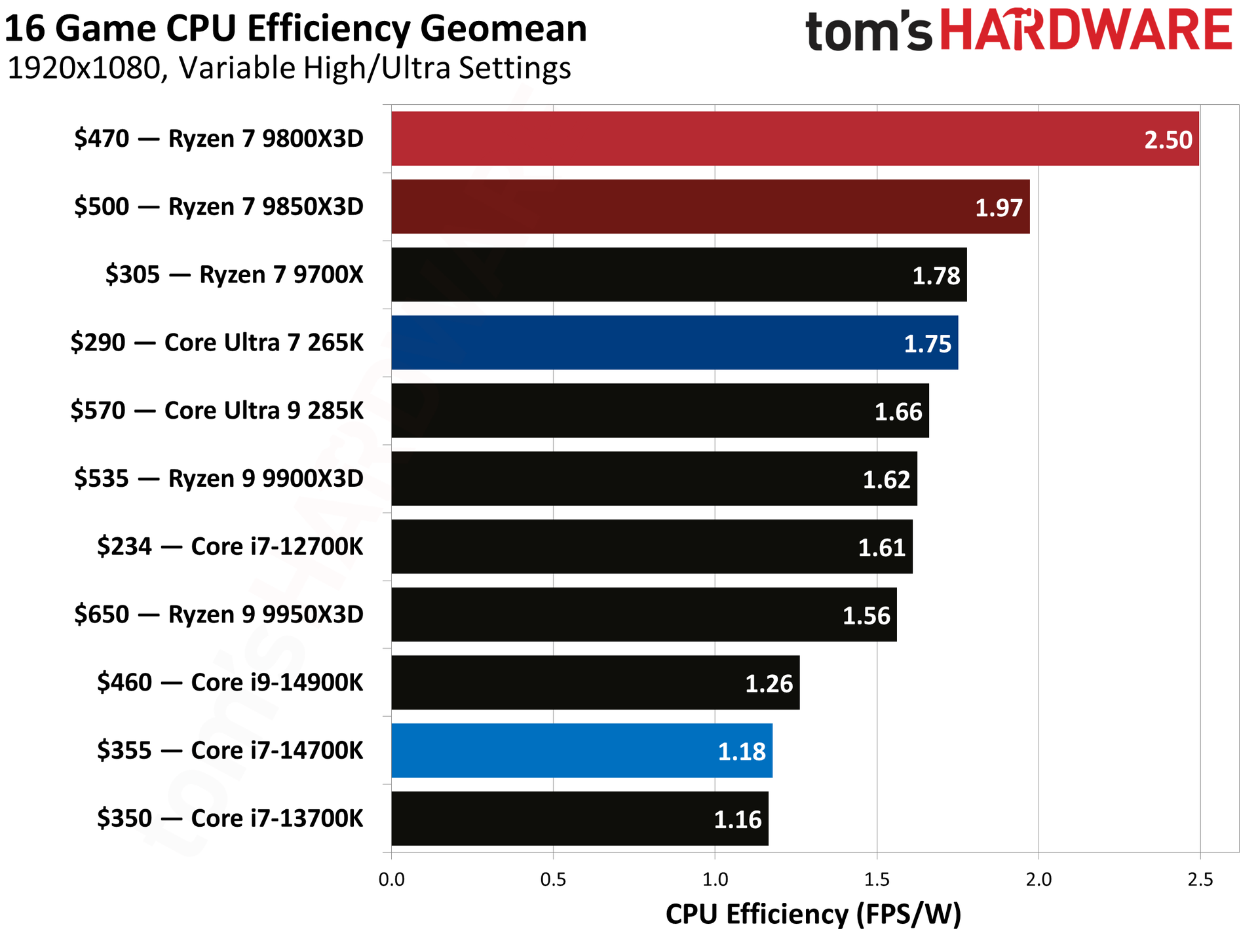
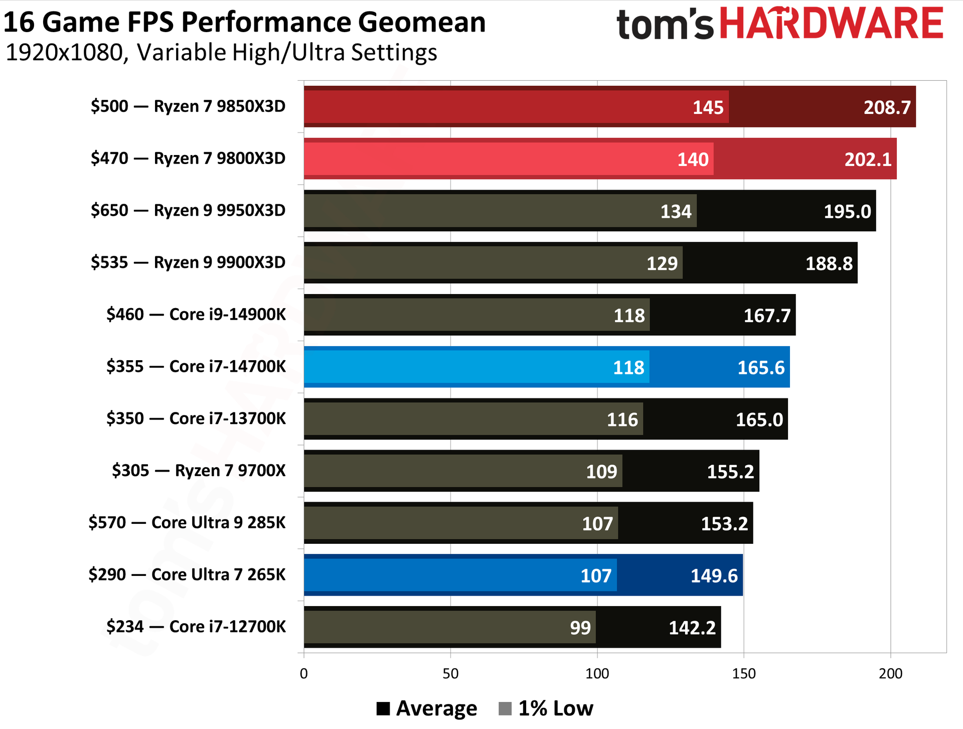
In our in-depth testing of the Ryzen 7 9850X3D, we found that it was only 3.3% faster than the Ryzen 7 9800X3D. But a win is a win, and that performance edge puts the CPU at the top of our 16-game 1080p FPS performance geomean, beating the more expensive Ryzen 9 9900X3D and 9950X3D. Although it loses out to Intel in some productivity workloads, the less complex 8-core configuration packed into a single CCD results in lower power draw. As you can see from our results, the peak power consumption is around 170W, making it much easier to cool.
With the included 240mm AIO liquid cooler, you should be able to keep the Ryzen 7 9850X3D well under control during gaming and moderate workloads, although it may run warmer under heavy multi-core workloads. At its sale price of $484, you’re paying less than its actual launch price while getting two useful extras at no additional cost. That makes this a worthwhile deal for anyone looking to build a high-end gaming PC around AMD’s gaming-focused platform.
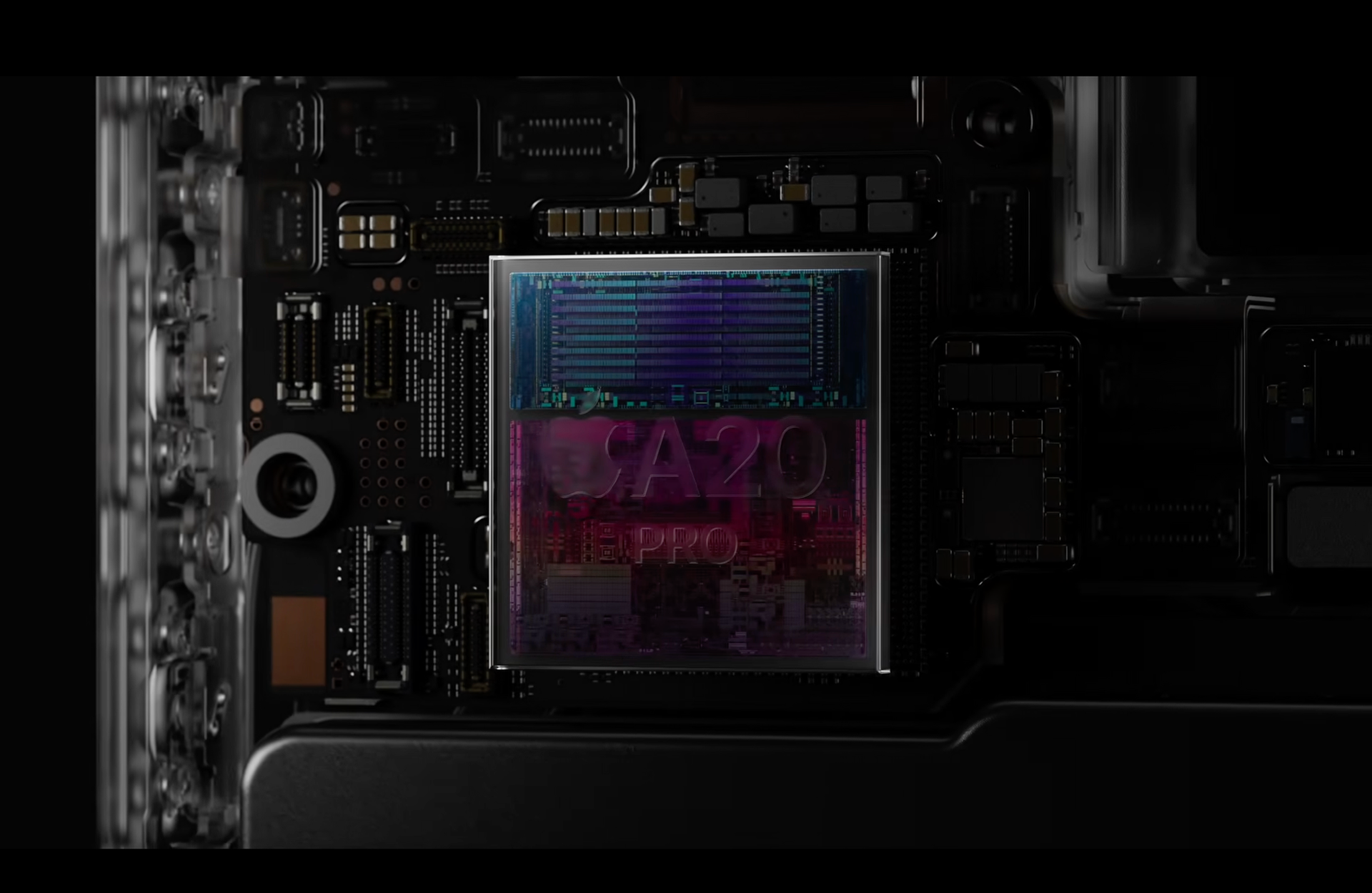
Architectural enhancements and significantly higher clock speeds enable Apple's A20 Pro application processor (AP), used in the company's latest iPhones, to deliver not only a substantial generation-to-generation performance boost but also to outperform leading desktop CPUs from AMD and Intel by up to a whopping 32% in the single-thread Geekbench 7 benchmark, setting the record for the highest single-thread performance. While high-end PC CPUs still have more oomph for multi-threaded workloads, the tiny A20 Pro is still faster than mainstream laptop CPUs even when many threads are involved.
Fastest smartphone SoC
A20 Pro
A19 Pro
A18 Pro
A17 Pro
A16 Bionic
General specifications
2P+4E, up to 4.93 GHz
2P+4E, up to 4.26 GHz
2P+4E, up to 4.0 GHz
2P+4E, up to 3.77 GHz
2P+4E, up to 3.46 GHz
Single-Thread
4006
3249
3082
2641
2405
Multi-Thread
11460
9016
8185
7050
6600
Apple's A20 Pro system-on-chip (SoC) delivers 4,006 points in single-thread and 11,460 points in the multi-thread Geekbench 7 benchmark, which represents a 23.3% higher ST performance and 27.1% higher MT performance compared to the immediate predecessor, the Apple A19 Pro, according to an early submission (which may or may not demonstrate performance of actual A20 Pro-based products, so take the results with a grain of salt).
Generation
Single-thread
Improvement
Multi-thread
Improvement
A16 Bionic
2,405
—
6,600
—
A17 Pro
2,641
9.80%
7,050
6.80%
A18 Pro
3,082
16.70%
8,185
16.10%
A19 Pro
3,249
5.40%
9,016
10.20%
A20 Pro
4,006
23.30%
11,460
27.10%
The new SoC delivers the highest generation-over-generation performance improvement for Apple's smartphone processors in years and is currently the highest-performing mobile AP. Furthermore, the A20 Pro beats AMD’s 16-core Ryzen 9 9950X3D by 26% and Intel’s Core i9-14900KS by 32% in single-thread performance.
A20 Pro
Snapdragon 8 Elite Gen5 (SM8850)
Xring O3
Exynos 2600 (S5E9965)
Dimensity 9400 (MT6991)
Tensor G5 (GS501)
Kirin 9050 Pro
General specifications
2P+4E, up to 4.93 GHz
2P+6E, up to 4.74 GHz
2X+4P+4E, up to 4.36 GHz
1X+3P+6E, up to 3.80 GHz
1X+3P+4A, up to 3.62 GHz
1X+5P+2E, up to 3.78 GHz
1X+2P+4E+2LP, up to 3.10 GHz
Single-Thread
4006
3047
2996
2694
2273
2011
1028
Multi-Thread
11460
10212
11777
10580
7745
5859
4794
When it comes to the single-thread Geekbench 7 benchmark, Apple's A20 Pro outperforms its closest rivals — Qualcomm's Snapdragon 8 Elite Gen5 (SM8850) and Xiaomi's XRing O3 — by 31.5% - 33.7%. In fact, both SM8850 and XRing O3 perform on par with Apple's two-years-old A18 Pro. The six-core A20 Pro also beats the eight-core SM8850 by 12.2% in multi-thread workloads in Geekbench 7 and offers roughly similar multi-thread performance to the 10-core XRing O3.
SoC
Single-thread
A20 Pro advantage
Multi-thread
A20 Pro advantage
A20 Pro
4,006
—
11,460
—
Snapdragon 8 Elite Gen 5
3,047
31.50%
10,212
12.20%
Xring O3
2,996
33.70%
11,777
−2.7%
Exynos 2600
2,694
48.70%
10,580
8.30%
Dimensity 9400
2,273
76.20%
7,745
48.00%
Tensor G5
2,011
99.20%
5,859
95.60%
Kirin 9050 Pro
1,028
289.70%
4,794
139.00%
Compared with other flagship smartphone processors, Apple's A20 Pro holds a commanding lead in Geekbench 7. It is 76% faster in single-thread and 48% faster in multi-thread performance than MediaTek's eight-core Dimensity 9400, while it nearly doubles the performance of Google's eight-core Tensor G5, with advantages of 99% and 96%, respectively. But the most striking gap of A20 Pro is with Huawei’s Kirin 9050 Pro: Apple's flagship is 290% faster in single-thread and 139% faster in multi-thread Geekbench 7 workloads.
A great laptop CPU
While Apple's A20 Pro continues to feature 'only' six cores like many generations before it, this time around the processor packs two 'super' desktop-class general-purpose cores running at up to 4.93 GHz, four efficiency cores running at lower clocks, and a memory interface that delivers +50% higher memory bandwidth compared to its predecessor (allegedly using a 96-bit memory I/O).
The architectural enhancements of advanced CPU cores running at nearly 5 GHz, along with a more capable memory subsystem, not only enable a massive generational performance uptick, but also allow the chip to offer unbeatable single-thread performance and massive multi-thread performance that is comparable to that of laptop CPUs, including previous-generation laptop CPUs from Apple.
A20 Pro
A19 Pro
M5
M4
M3
Ryzen 9 9950X3D
Core i9-14900KS
Core Ultra X9 388H
Core Ultra 5 325
Core Ultra 5 332
General specifications
2P+4E, up to 4.93 GHz
2P+4E, up to 4.26 GHz
4S+6E, up to 4.6 GHz
4P+6E, up to 4.40 GHz
4P+4E, up to 4.05 GHz
16P/32T, 4.30 GHz - 5.75 GHz
8P+16E/32T, 3.20 GHz - 6.0 GHz
4P+8E+4LP/16T, up to 5.1 GHz
4P+0E+4LP, up to 4.6 GHz
2P+0E+4LP, up to 4.40 GHz
Single-Thread
4006
3249
3739
3351
2808
3182
3024
2694
2297
2134
Multi-Thread
11460
9016
18671
15806
12061
30428
21145
18121
11107
6976
Indeed, Apple's A20 Pro is 7% faster than M5, 20% faster than M4, and 43% faster than M3 in single-thread performance. Its six-core design cannot match its multi-thread performance, trailing the 10-core M5 by 39% and the 10-core M4 by 27%. Yet, it is only 5% behind the eight-core M3.
Processor
ST score
A20 Pro ST advantage
MT score
A20 Pro MT advantage
A20 Pro
4,006
—
11,460
—
A19 Pro
3,249
23.30%
9,016
27.10%
Apple M5
3,739
7.10%
18,671
−38.6%
Apple M4
3,351
19.50%
15,806
−27.5%
Apple M3
2,808
42.70%
12,061
−5.0%
Ryzen 9 9950X3D
3,182
25.90%
30,428
−62.3%
Core i9-14900KS
3,024
32.50%
21,145
−45.8%
Core Ultra X9 388H
2,694
48.70%
18,121
−36.8%
Core Ultra 5 325
2,297
74.40%
11,107
3.20%
Core Ultra 5 332
2,134
87.70%
6,976
64.30%
When compared to Intel's Panther Lake, the A20 Pro is 48.7% faster in single-thread performance than the flagship Core Ultra X9 388H, yet the 16-core Panther Lake processor is 63% faster in multi-thread workloads. Against lower-end Panther Lake parts, the A20 Pro is 74% – 88% faster in ST workloads and even leads the Core Ultra 5 325 and Ultra 5 332 by 3% and 64%, respectively, in multi-thread benchmarks.
The particularly striking results of Apple's A20 Pro are the 26% – 33% single-thread advantage over flagship AMD and Intel desktop CPUs, though the desktop processors remain dramatically faster in multi-thread workloads.
First 2nm smartphone SoC
When Apple transitioned to TSMC's N3B (3nm-class) process technology from N4 (4nm-class) with its A17 Pro SoC back in 2023, the new processor was barely 9.8% faster in ST and 6.8% faster than its predecessor A16 Bionic. By contrast, with its first 2nm smartphone SoC made on TSMC's N2 node, Apple offers a massive performance boost over the A19 Pro produced on N3P.
(Image credit: Apple)
Indeed, Apple's A19 Pro packs two 'desktop-class' 'super cores' whose design is 'driven in part by increased front-end bandwidth, a new cache hierarchy, and enhanced branch prediction,' as Apple described its 'super cores' inside the M5 processor earlier this year. Such architectural enhancements obviously massively increase performance in single-thread workloads at the cost of increased die size, transistor count, and power. Apparently, N2 enabled Apple's designers to squeeze two desktop-grade CPU cores into a smartphone SoC.
Speaking of M5, it is noteworthy that A20 Pro delivers 7.1% higher single-thread performance than M5 while running at a clock speed that is 7.1% higher than that of M5, which is probably a good indicator that Apple's A19 Pro uses the same 'super cores' as M5.
While some may consider using PC-grade general-purpose CPU cores in a smartphone chip an overkill, Apple is known for using and supporting PC technologies in its mobile SoCs (NVMe, PCIe, DisplayPort-over-USB-C, hardware virtualization, etc.). Keeping in mind that Apple also uses A-series SoCs inside iPads and inexpensive laptops, it makes a great sense to have these technologies in its smartphone application processors. With desktop-grade cores inside the A20 Pro, the company greatly expands use cases of these CPUs while also solidifying their position in traditional segments that they will address in the coming quarters.
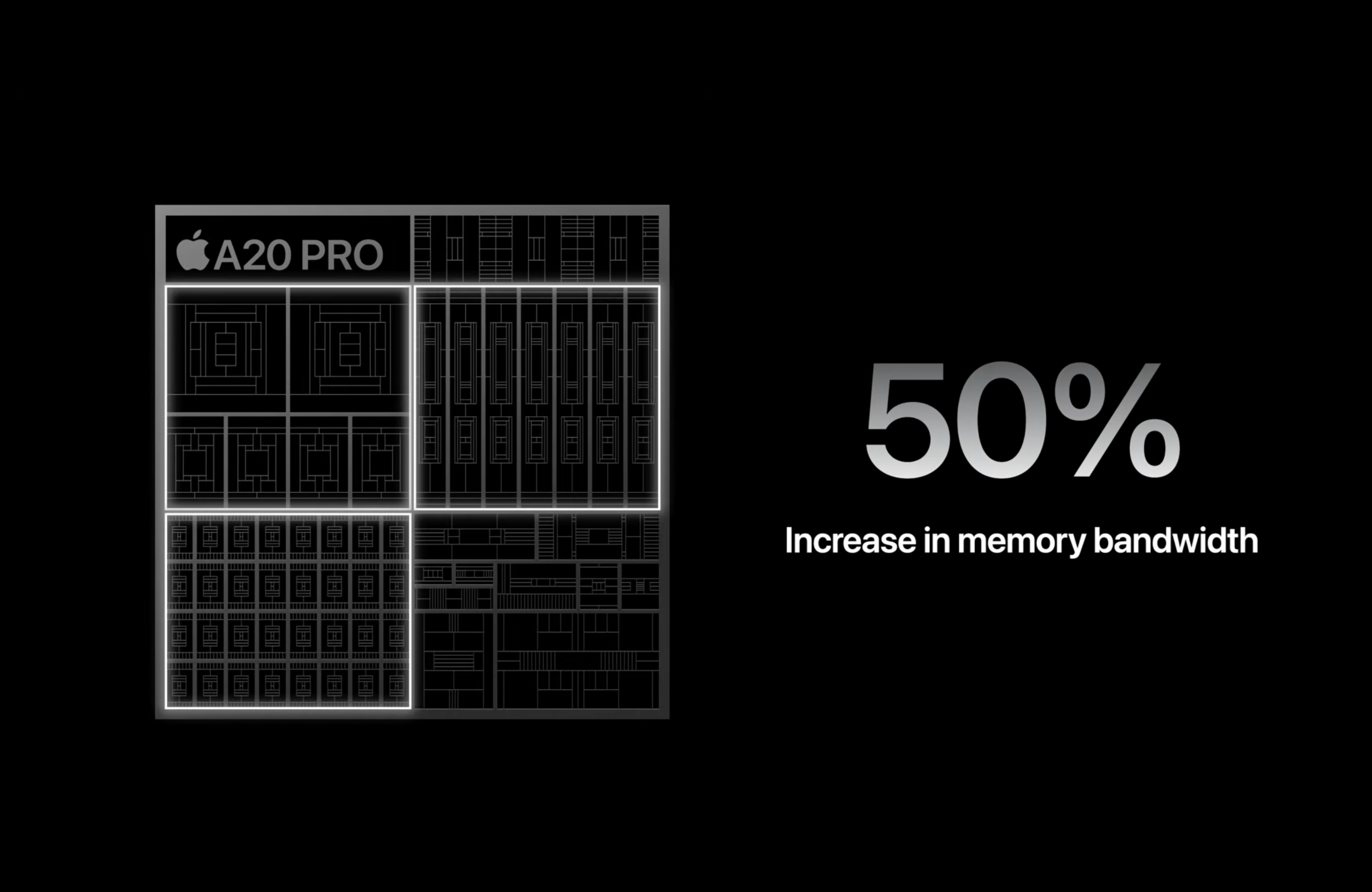
Without any doubts, Apple's transition to TSMC's N2 starts with a massive general-purpose performance increase, driven by 'fat' super cores and a memory subsystem featuring 50% more bandwidth compared to the A19 Pro. Over the next few weeks, we are also going to learn how Apple upgraded the GPU, NPU, and other aspects of the A20 Pro, and we are going to find out whether the upgrades are as impressive or incremental. In any case, so far, the A20 Pro looks very good.
AMD has officially launched the Ryzen 5 5500F and Ryzen 5 7500, two strong contenders for the best CPUs on the market if you're on a budget. Both are hexa-core chips, with the Ryzen 5 5500F featuring AMD's Zen 3 execution cores and the Ryzen 5 7500 using the newer Zen 4 execution cores. The Ryzen 5 5500F and Ryzen 5 7500, priced at $99 and $189, respectively, are available at U.S. retailers starting today.
The Ryzen 5 5500F, despite its similar model name to the Ryzen 5 5500, belongs to a different family in AMD's portfolio. The Ryzen 5 5500F hails from the Ryzen 5000 series (codenamed Vermeer), which uses a multi-chiplet architecture. Meanwhile, the Ryzen 5 5500 comes from the Ryzen 5000G series (codenamed Cezanne), which uses a monolithic die design.
Therefore, it is more sound to call the Ryzen 5 5500F a lower-binned version of the Ryzen 5 5600, rather than an iGPU-less variant of the Ryzen 5 5500, which lacks integrated graphics to begin with. The distinction matters because the Ryzen 5 5500F is closer to the Ryzen 5 5600, albeit with a 500 MHz lower boost clock speed and half the L3 cache.
The Ryzen 5 5600, which launched at $199, now retails for around $159, making the new Ryzen 5 5500F approximately 38% more affordable. Meanwhile, the Ryzen 5 5500, which debuted at $159, has lost substantial value over the years. OEM tray versions of the Ryzen 5 5500 now start at just $74, so it is still the most cost-effective entry point into the AM4 ecosystem. Compared to the Ryzen 5 5500, the Ryzen 5 5500F carries a 34% price premium. The latter justifies its higher cost with a slightly higher boost clock speed, which translates to better gaming performance, and support for PCIe 4.0, unlocking faster SSDs and graphics cards.
Ryzen 5 5500F and Ryzen 5 7500 Specifications
Processor
MSRP / Current Price
Architecture / Codename
Platform
Cores / Threads
Base / Boost Clock (GHz)
L2 Cache (MB)
L3 Cache (MB)
Graphics Model
Graphics Core
Graphics Frequency (MHz)
Memory Support
PCIe Lanes
TDP (W)
Ryzen 5 7600
$229 / $226
Zen 4 / Raphael
AM5
6 / 12
3.8 / 5.1
6
32
AMD Radeon
2
2,200
DDR5-5200
24 PCIe 5.0
65
Ryzen 5 7500
$189 / $189
Zen 4 / Raphael
AM5
6 / 12
3.7 / 5.0
6
32
AMD Radeon
2
2,200
DDR5-5200
24 PCIe 5.0
65
Ryzen 5 7500F
$179 / $157
Zen 4 / Raphael
AM5
6 / 12
3.7 / 5.0
6
32
N/A
N/A
N/A
DDR5-5200
24 PCIe 5.0
65
Ryzen 5 5600
$199 / $159
Zen 3 / Vermeer
AM4
6 / 12
3.5 / 4.4
3
32
N/A
N/A
N/A
DDR4-3200
20 PCIe 4.0
65
Ryzen 5 5500F
$99 / $99
Zen 3 / Vermeer
AM4
6 / 12
3.0 / 4.4
3
16
N/A
N/A
N/A
DDR4-3200
20 PCIe 4.0
65
Ryzen 5 5500
$159 / $74
Zen 3 / Cezanne
AM4
6 / 12
3.6 / 4.2
3
16
N/A
N/A
N/A
DDR4-3200
20 PCIe 3.0
65
When it comes to the Ryzen 5 7500, little mystery surrounds its place in AMD's product stack. True to its name, the Ryzen 5 7500 is the same processor as the Ryzen 5 7500F, which launched three years ago, but with integrated Radeon graphics. This small addition suits users who need basic display output and do not plan to spend money on a discrete graphics card. Apart from the integrated graphics, all core specifications remain identical between the two models.
As a result, the difference between the Ryzen 5 7600 and the Ryzen 5 7500 stands. The former boasts a 100 MHz higher base and boost clock, so performance is somewhat better in certain processor-intensive workloads or gaming scenarios. However, most users may not notice the difference.
The Ryzen 5 7500F hit the market at $179, but over time its retail price has dropped to about $157. In contrast, the Ryzen 5 7600 has held its value over the years, falling only slightly from its original MSRP of $229 to around $226. As a result, the Ryzen 5 7500 positions itself as a mid-point option, priced 16% lower than the Ryzen 5 7600 and 20% above the Ryzen 5 7500F.
The Ryzen 5 7500 makes sense in this market because not everyone is a gamer, so integrated graphics mean you do not have to spend a fortune on a discrete graphics card at today's ridiculous prices. However, because it runs on AMD's AM5 platform, the Ryzen 5 7500 is still bound by the sky-high cost of DDR5.
We reported on the new Apple A20 Pro system-on-a-chip (SoC) for smartphones yesterday, an integral attraction within Apple’s first foldable, the iPhone Duo, and in the iPhone 18 Pro devices. Now the first A20 Geekbench 6 benchmark results are starting to pop up online, and they’re very impressive, particularly in single-core performance. If the result spotted by Longhorn is a typical one, the 4,719 single-core and 12,677 multi-core scores mean the new A20 is around 25% faster than its predecessor. Its single-core score can also make some of the best PC CPUs look anemic.
huhApple A20 Pro Geekbench 6 numbers 🫠https://t.co/py5rdZ1ekk pic.twitter.com/Snrn9lTks9September 10, 2026
Apple’s official performance claims are interesting, as usual, but we’re always happy to see the third-party performance indicators start to emerge ahead of independent reviews. Heralding its new 2nm silicon yesterday, Apple might have actually understated the boost the A20 can deliver, with the official line about this “desktop-class” processor being the “fastest CPU in a smartphone,” and a claim that it is ‘just’ 20% faster than the previous gen. However, Geekbench isn’t the best indicator of real-world performance, and this is just a sample of one to sprinkle salt upon.
What are numbers without relevant comparisons, though? For more perspective on Apple’s newest silicon, which might also be thrown into a new Neo laptop (or desktop) in the coming months, check out the table below.
Above, we’ve pitted the Apple A19 Pro from last year’s iPhone 17 Pro as the second comparison column entrant. Apple has worked on multiple angles to deliver improvements over last year. It says that it has both new super-cores and efficiency cores in play. Then there’s the refined 2nm process and the faster clocks, too.
For some wider context, we’ve also tabulated one of Apple’s newest M5 computer chips, a modern Qualcomm Snapdragon Elite X2 laptop chip, and the AMD Ryzen 9 9950X3D2, for a fun desktop PC angle. Less fun is the comparison with the Asus Zephyrus G16 2024 laptop I’m using now, with an AMD Ryzen AI HX 370 chip. Its Geekbench 6 scores of roughly 2,800 / 14,500 are easily outclassed by Apple’s new smartphone processor in 1T tests, but retain a little dignity by winning by ~1,800 points in nT tests.
Apple is opening up pre-orders for its new iPhones with A20 silicon shortly, with retail release on Friday, September 18. It usually lifts review embargoes a few days before retail. We should therefore see a broader range of benchmarks and tests from good sources in the coming week.
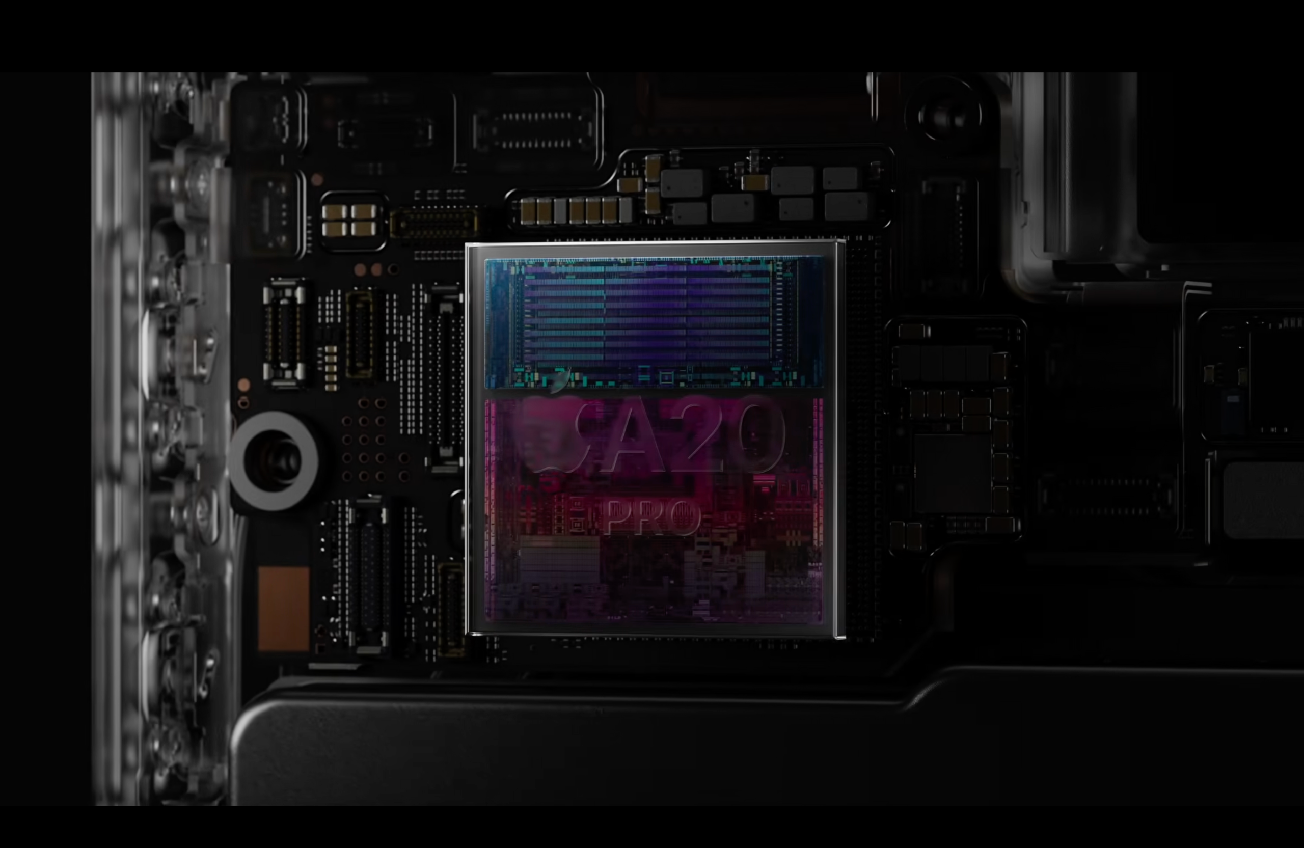
Apple has a new top system-on-a-chip for smartphones, the A20 Pro. The new processor debuted at Apple's iPhone event today — the first event led by newly minted chief executive officer John Ternus — alongside a new in-house modem (the C2).
The A20 Pro is Apple's first 2-nanometer chip in an iPhone. (Its first-ever 2 nm chip is the M6, which the company announced in August and which will debut in the Mac Mini later this month). Like the M6, the A20 features dual neural engines, new CPU and GPU cores.
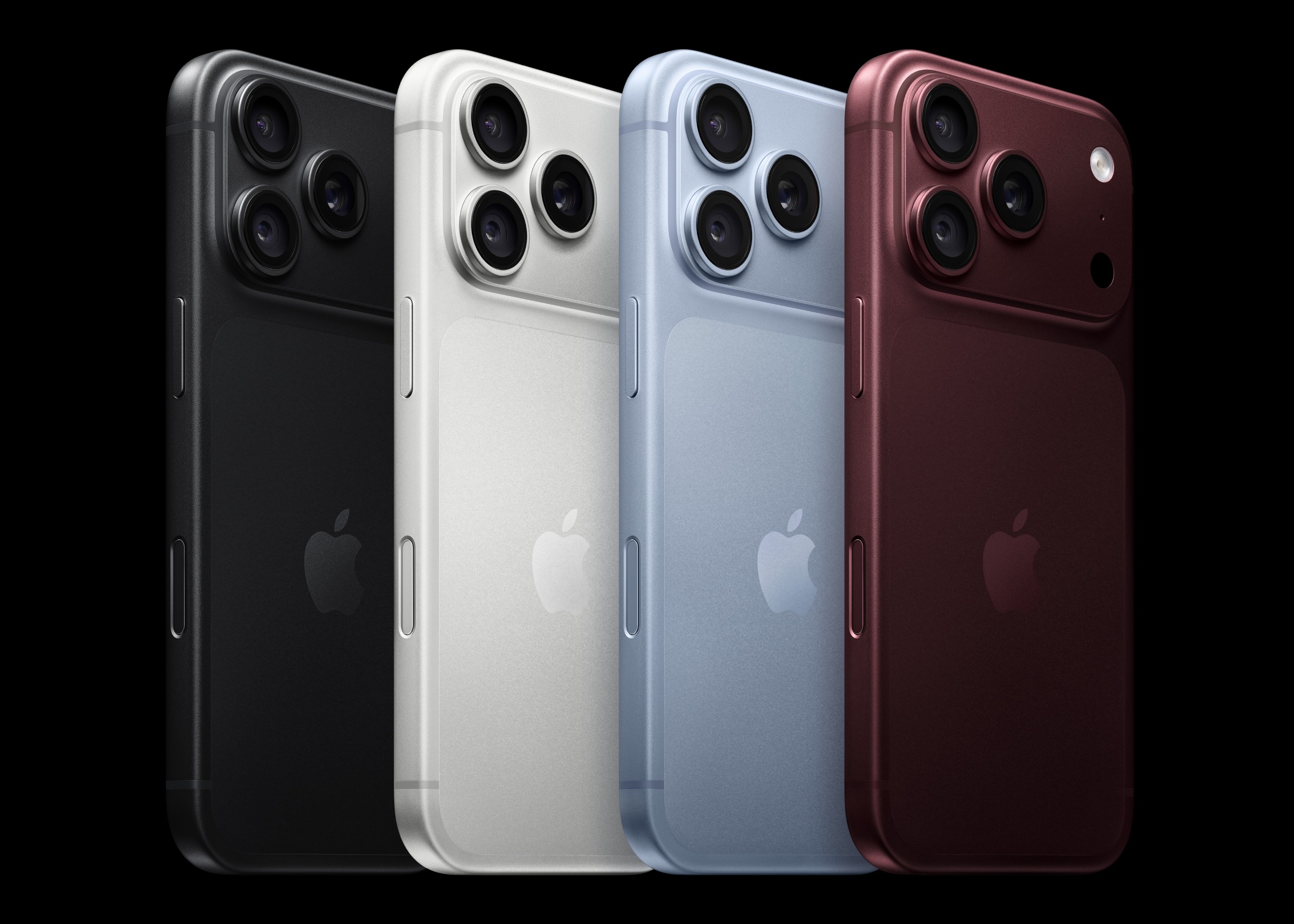
The A20 Pro will power the new foldable iPhone Duo, along with the iPhone 18 Pro and Pro Max.
AppleAppleAppleAppleAppleApple
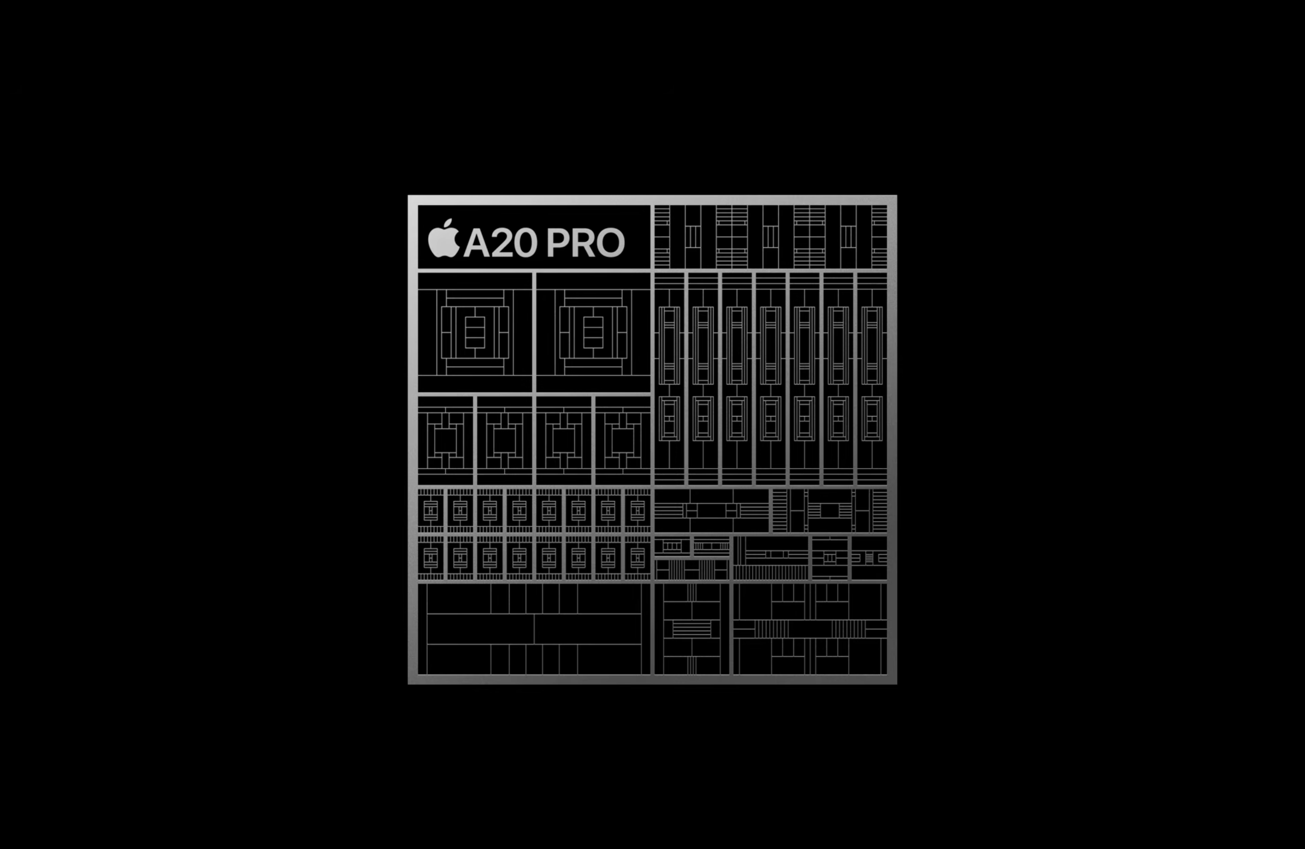
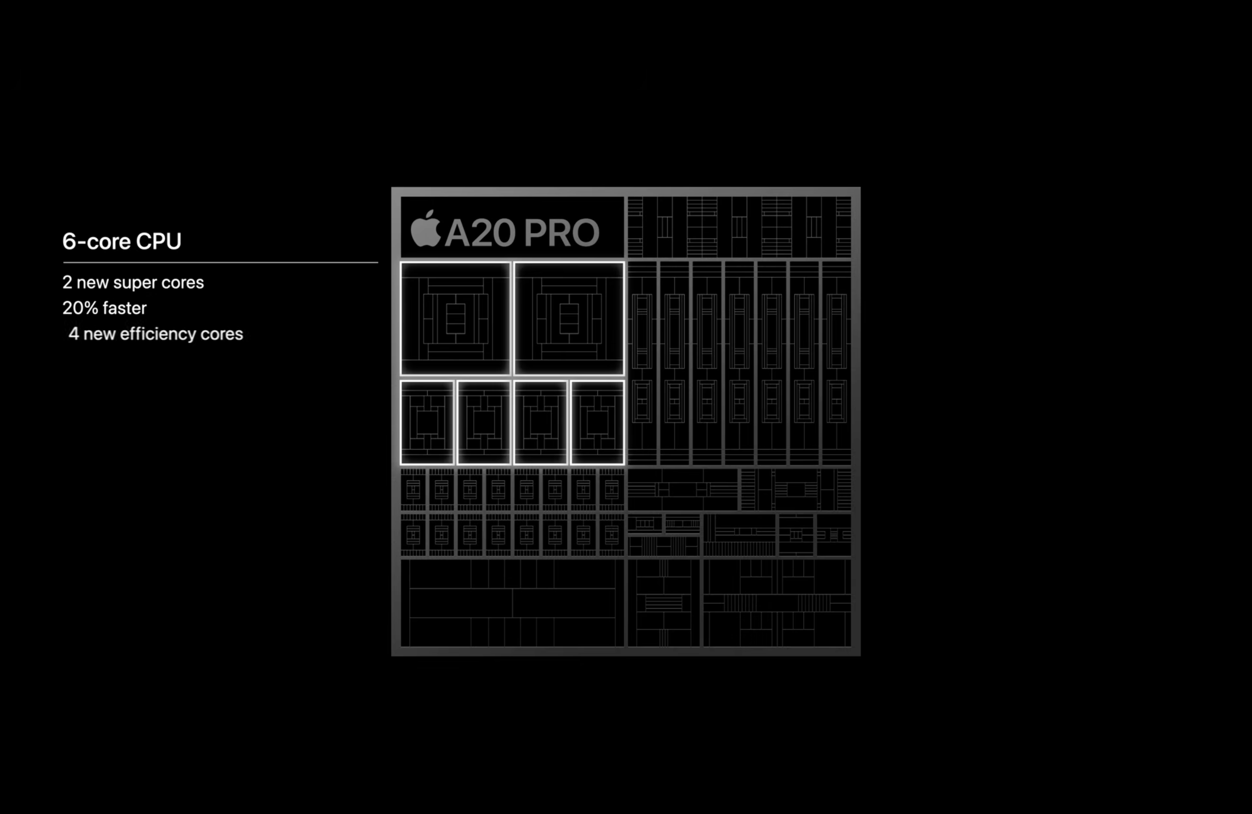
The new SOC boasts a 6-core CPU with two of the company's super-cores (20% faster than last generation), and there are also four efficiency cores with neural accelerators. Apple is calling this a "desktop-class" processor and the "fastest CPU in a smartphone."
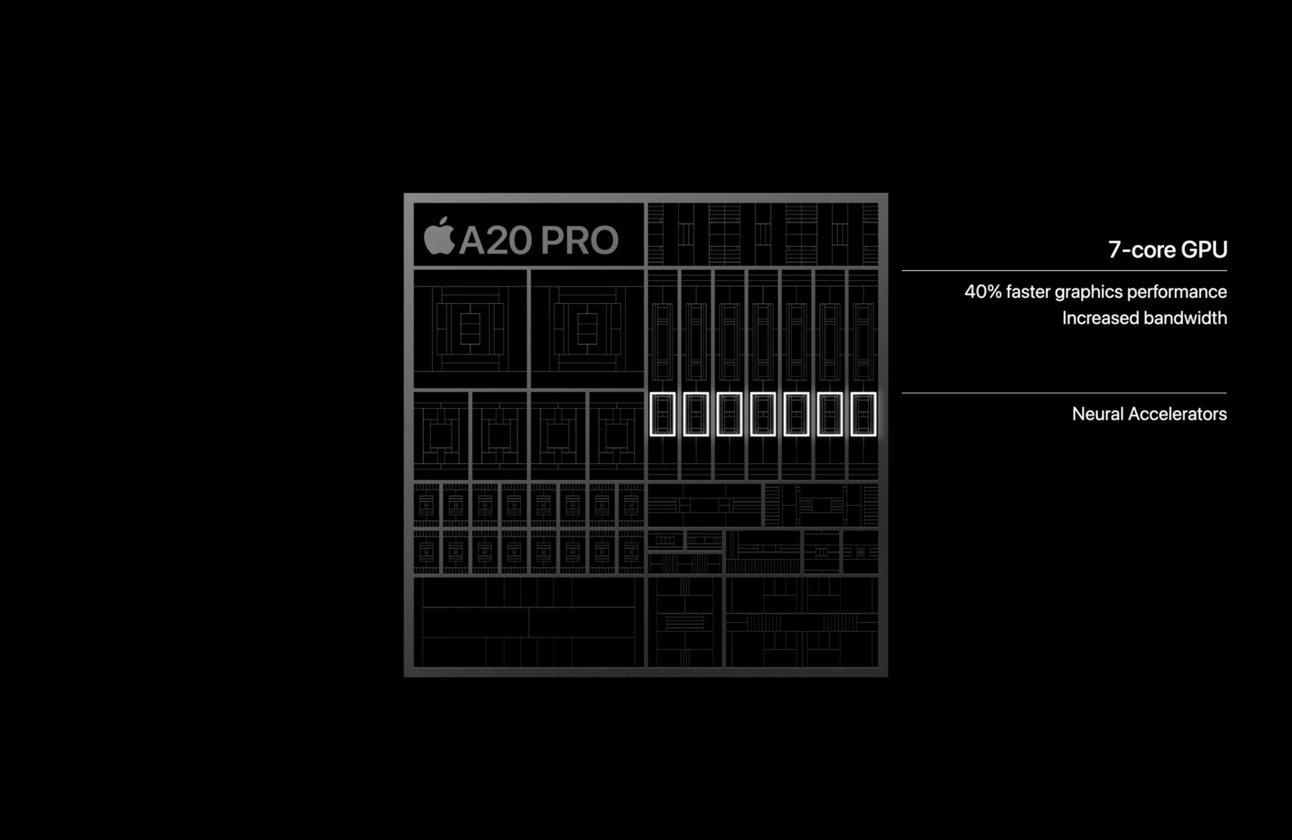
The 7-core GPU has a 40% boost gen-over-gen with increased bandwidth, along with new neural accelerators that the company says allows for twice-as-fast FP8 compute.
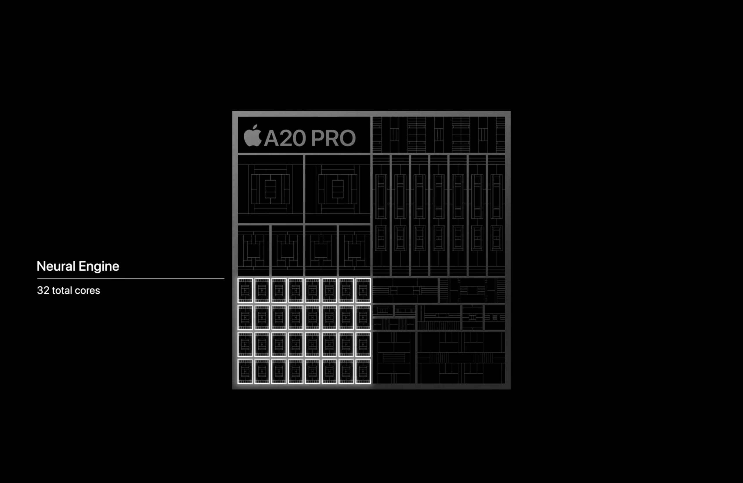
The two neural engines have a combined 32 total cores. There's a 50% increase in memory bandwidth on the chip, which Apple says is the widest memory interface in an iPhone.
Apple has also changed the packaging, with the silicon dies placed in a way that removes memory from the thermal path of the SOC, allowing the silicon to attach directly to the vapor chamber. That vapor chamber has a three times larger surface area over the 17 Pro, and also includes more graphite and copper along with 80% recycled stainless steel.
The company claims that this will allow for up to 40% sustained performance over the iPhone 17 Pro and 2x sustained performance over the 16 Pro.
Apple says that A20 Pro's efficiencies and new battery designs allow for better longevity. The company claims the Pro will get 36 hours of video playback, and 45 hours on Pro Max video. Using a proprietary test based on data from how people use their phones, Apple claims 24 hours per charge on the 18 Pro and 30 hours on the Pro Max.
(Image credit: Apple)
Beyond the SOC, Apple is also using a new C2 cellular modem, replacing Qualcomm. Apple claims that C2 "delivers meaningfully faster uploads when compared to C1X while consuming 15 percent less energy," and also adds mmWave support in the United States. Both phones also feature the N1 networking chip for Wi-Fi 7, Bluetooth 6, and Thread.
The iPhone 18 Pro will start at $1,199, while the Pro Max will start at $1,299. The phones will be available on September 18. The phones also feature an updated Dynamic Island and a 48-megapixel fusion camera with a variable aperture, plus customizable settings such as white balance and cinematic effects that can be added after capture.
(Image credit: Apple)
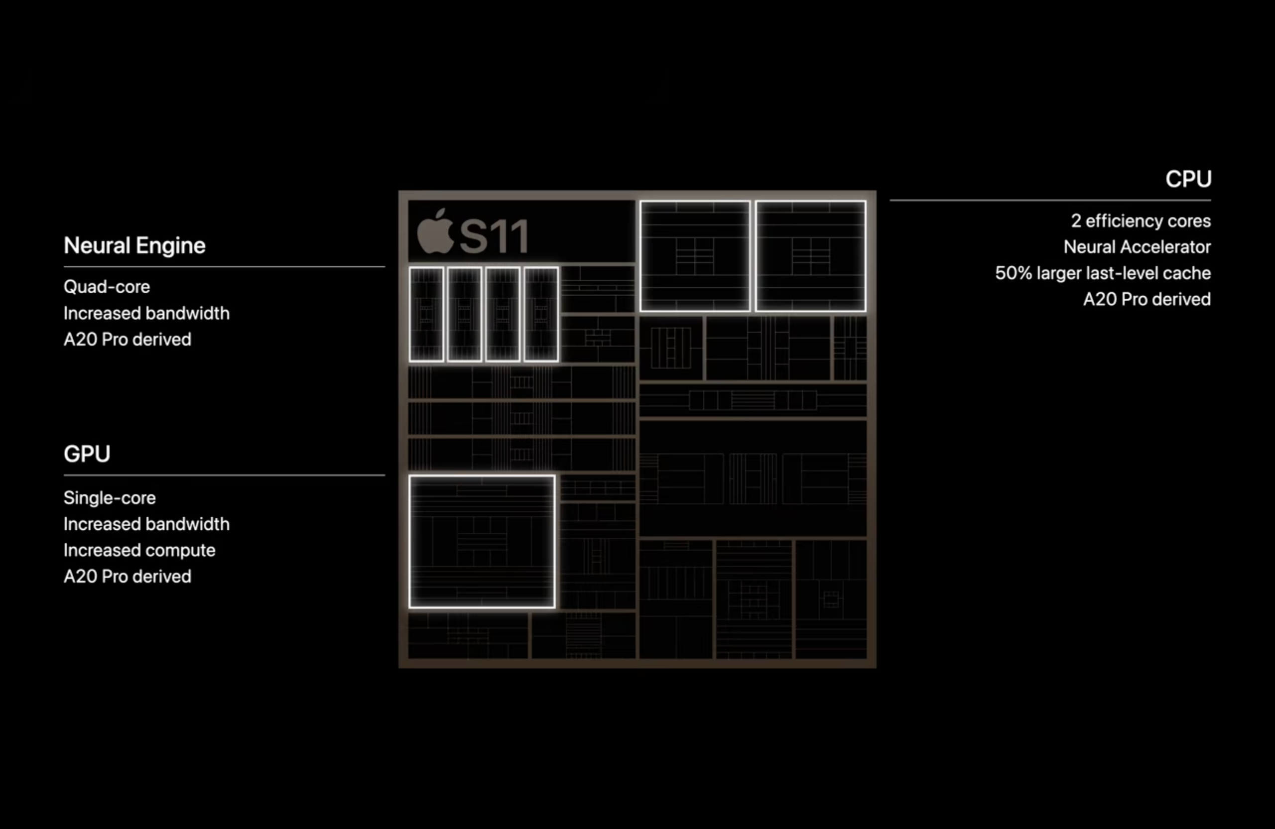
Apple's other new silicon was the S11, a chip for the Apple Watch Series 12 and Ultra 4.
iPhone Duo
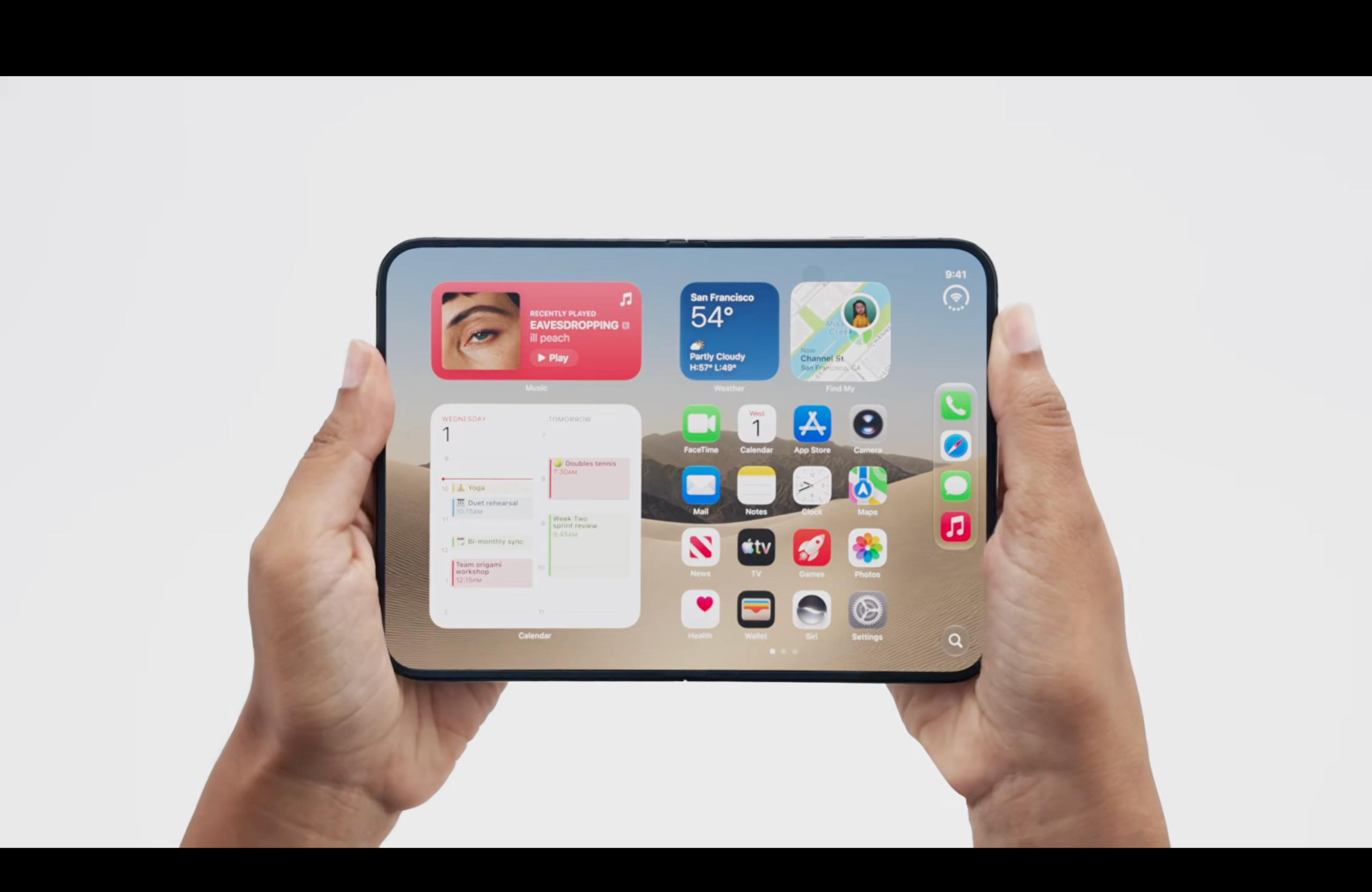
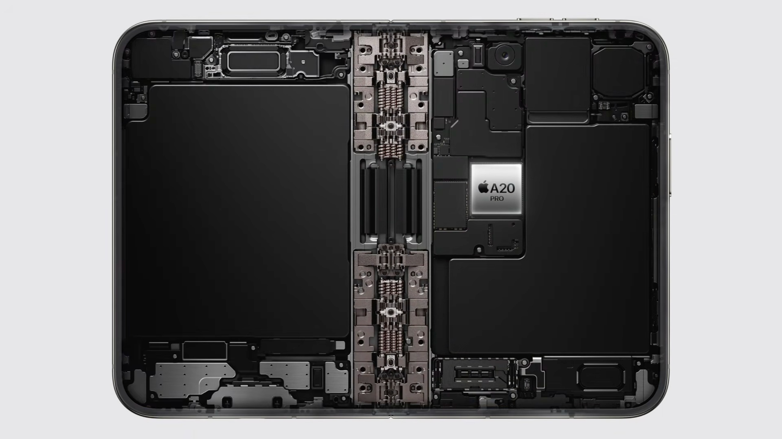
The iPhone Duo, Apple's long-awaited foldable phone, will also use the A20 Pro.
AppleAppleApple
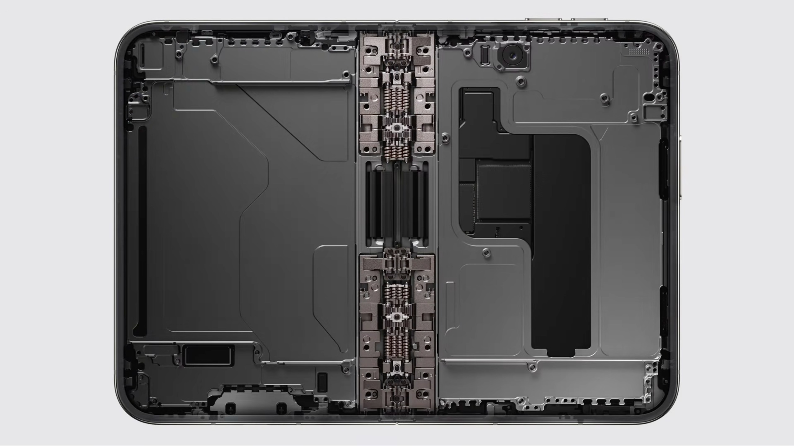
The foldable will be Apple's first phone with a FaceTime camera behind the display, and Apple detailed the hinge and aerospace-grade titanium construction. The Duo is IP68-rated for dust and water resistance. It comes in "star white," as well as "night sky" (a dark blue).
The OS, iOS 27, will allow for docks and controls to live on the sides of the system, putting them near your hand. When opened, it's the thinnest iPhone ever and has the largest screen on an iPhone at 7.6 inches. Later this year, Apple Pencil will be supported on the Duo on both screens.
AppleApple
Apple will use Touch ID for biometrics, jettisoning the Face ID from more recent slab-style phones. Apple said this is the best way to go because it's available whether open or closed, and you can enroll multiple fingers.
The phone supports multiple "poses," including partial folds, and a standby mode when used in a tent-style pose — even when it's not charging.
Apple's internal display has an anti-glare display to "minimize crease visibility," which the company also claims feels premium under your fingers, with a titanium plate supporting the panel, along with a hinge with over 100 components. Samsung also released a phone with a minimal crease in the Galaxy Z Fold 8 earlier this year, but we'll have to see how reviewers compare the two screens.
AppleAppleApple
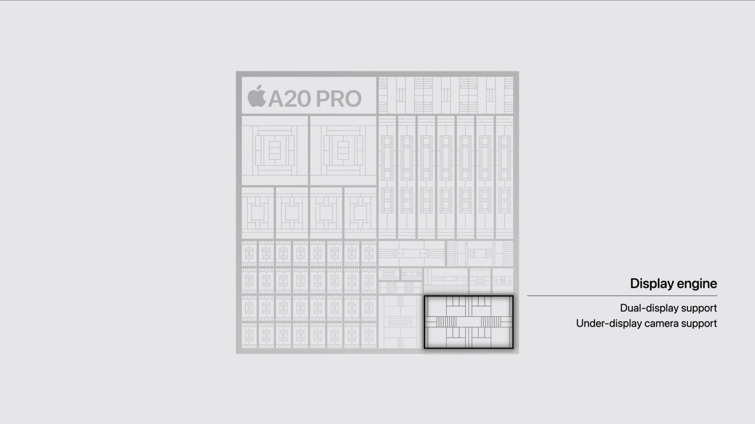
A20 Pro has a new display engine that supports both displays. Like the 18 Pro and 18 Pro Max, Apple is using the C2 cellular modem over Qualcomm's in the iPhone Duo.
The iPhone Duo is eSIM-only everywhere in the world, maximizing battery space. Each side of the phone has its own battery, which operates as one with software. Apple is claiming up to 31 hours of video playback on the inner display and 44 hours on the outer display. Using its own model, Apple claims 24 hours when using "both screens equally."
The phone has a two-camera system. The main camera is a 48MP lens with up to 2x telephoto, while the other is an ultrawide lens. The 48MP camera is the same one on the 18 Pro, though without the variable aperture. The center-stage camera on the front is a 12MP camera. The inner display has an under-screen FaceTime camera.
The iPhone Duo starts at $1,999 for 256GB, and goes up to 2TB. Pre-orders start on October 16, and the phone will launch on October 23.
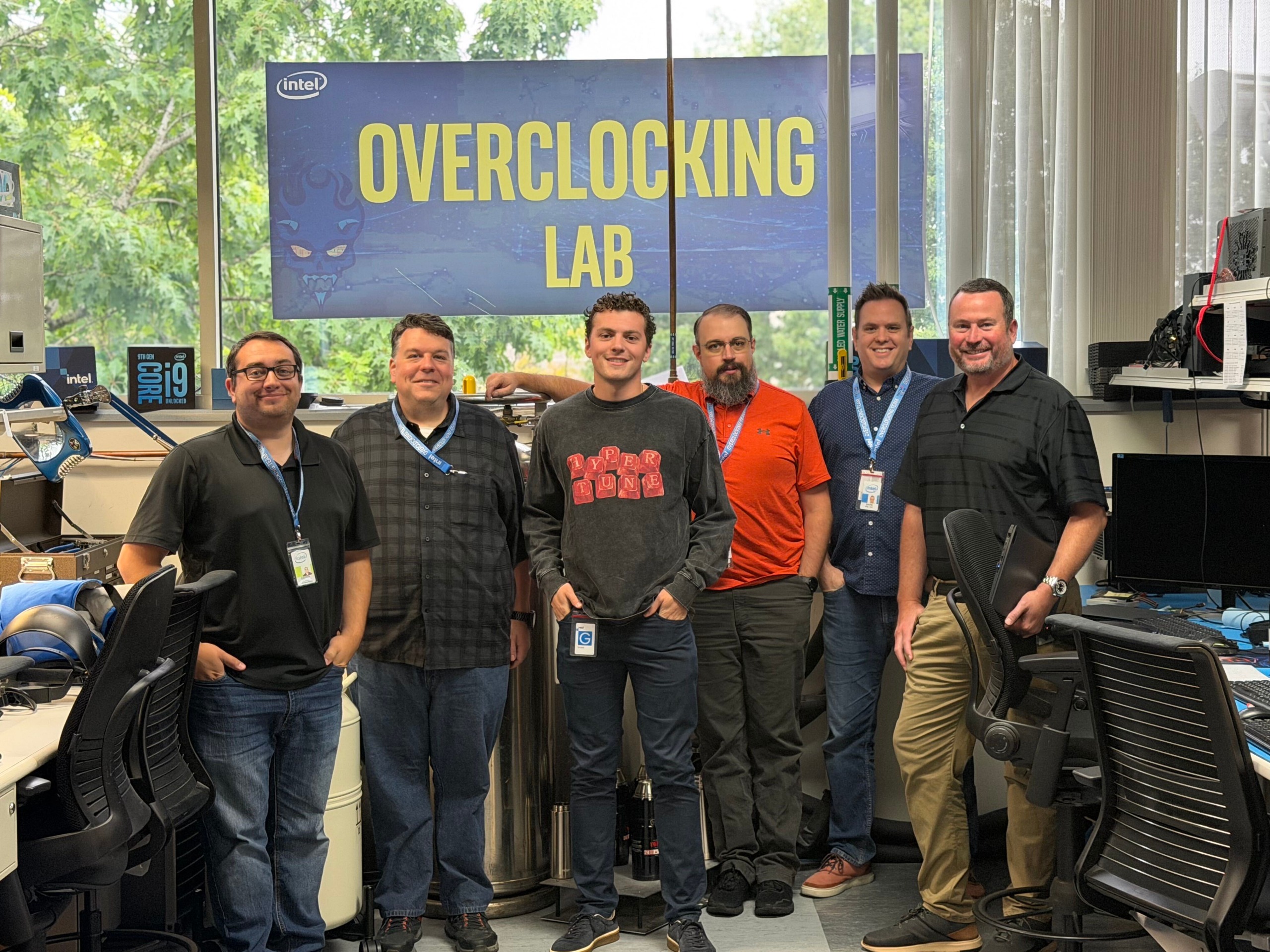
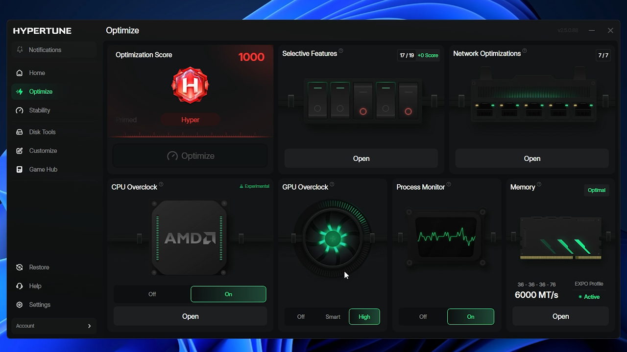
Following an early access period that included over 60,000 participants, auto-overclocking tool Hypertune has released its Gaming Performance Engineering platform, which is built on top of Intel's Extreme Tuning Utility (XTU) SDK and developed in partnership with Intel. The company claims the utility can boost frame rates by up to 60%, though you shouldn't expect that as the norm. The tool includes automated CPU and GPU overclocking, as well as customizable Windows features, network optimization, and game-specific optimizations.
Hypertune partnered with Intel to build the tool, which the company says "evaluates each supported system individually" before optimizing rather than relying on generalized profiles. In its press release, Hypertune says it collaborated with famed overclocker SkatterBencher (Pieter Plaisier) to refine the software. We've reached out to Plaisier to confirm their involvement.
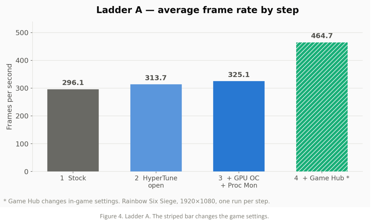
Automated tuning programs usually don't work as well as advertised, and we haven't had the chance to test Hypertune ourselves yet. Especially on more recent hardware, expect performance gains to be minor. Hypertune shared some of its internal benchmarks to back up the claim, showcasing the actual test systems it used, the numbers it gathered, and what each step of Hypertune contributed to the performance increase.
(Image credit: Hypertune)
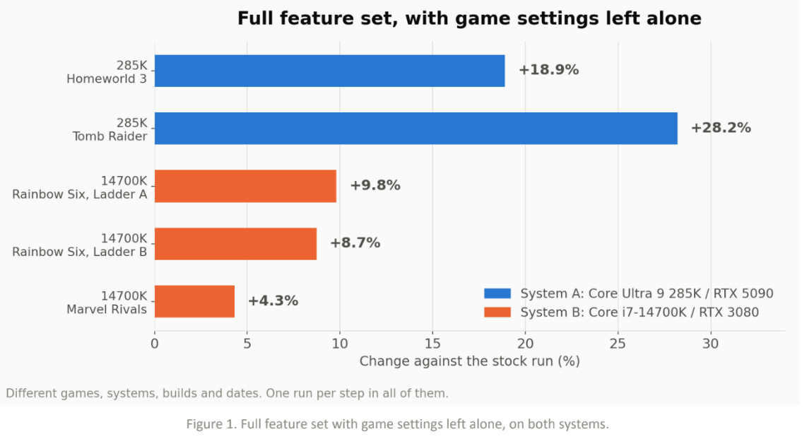
Hypertune tested two systems: one with a Core Ultra 9 285K and an RTX 5090, and another with a Core i7-14700K and an RTX 3080. For the 285K system, the team saw an 18.9% improvement in Homeworld 3 and a 28.2% improvement in Tomb Raider. For the 14700K system, the boost was up to 9.8% in Rainbow Six Siege and 4.3% in Marvel Rivals.
Notably, these results are with Hypertune's Game Hub disabled. Game Hub automatically applies a graphics settings profile to select games, leading to massive increases in performance. Naturally, tweaking your own graphics settings in the same way leads to the same result.
(Image credit: Hypertune)
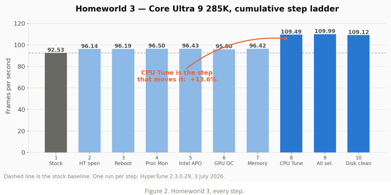
In Homeworld 3, you can see how each step in the process impacted performance, with CPU tunning contributing the single biggest increase in performance. As shown by Marvel Rivals in Hypertune's data, some games will see little to no benefit from Hypertune, though select titles with certain hardware may see a significant performance increase. In this case, the Core Ultra 9 285K has plenty of room for overclocking, and Homeworld 3 is particularly sensitive to the CPU, so the uplift makes sense.
(Image credit: Hypertune)
Elsewhere, the gains aren't as pronounced. In Rainbow Six Siege, you can see that Hypertune contributed about a 9.8% jump in performance, though the vast majority of the improvement comes through Game Hub, where Hypertune changes in-game settings.
In a press release, Hypertune founder Austin Copeland wrote that the team was "not trying to build a tool for overclockers," suggesting it's aimed toward users who may not know about specific settings (i.e., the Balanced power plan on dual-CCD X3D CPUs, or HAGS for DLSS Frame Generation). Copeland was previously a coach for eSports organization TSM, coaching Valorant teams under the name "Apex."
(Image credit: Hypertune)
Hypertune works through Intel's XTU SDK, and the company says its optimizations are non-destructive and fully reversible. The software is mainly targeted toward competitive titles (naturally, given Copeland's background), but it can apply optimizations globally across the system. Hypertune says it's safe to use with anti-cheat software, including Riot Vanguard, Easy Anti-Cheat, and BattlEye.
Although there are plenty of free tools that claim to optimize your system, Hypertune isn't among them. It's a subscription service, available for either $9.99 per month or $59.99 per year. In addition to software, Hypertune offers its "expert tuning" service for $80, where a technician will remote into your machine and manually tune it. On the subscription front, Hypertune offers a 7-day free trial.
Hypertune looks like one of the more robust automated overclocking tools we've seen, but it's worth highlighting that, in most cases, these tools don't do anything you can't accomplish yourself. If you're looking for a starting point, make sure to read our guides on how to overclock your graphics card and how to overclock your CPU.
Intel is reportedly set to hike CPU prices by 10%, according to a new Digitimes report. Citing supply chain sources, the outlet says the increase follows two others, one in the first quarter of 2026 and another in July, among some server and client CPUs. Notably, the sources didn't say which products the price increase applies to, though presumably, the increases would come through Intel's mobile and server businesses before desktop client. Citing industry sources, DigiTimes also reports that Intel is set to launch "major annual products" in March 2027, with AMD following up with launches of its own between June and July.
The increases come on the back of Intel seeking higher gross margins for its products as the PC market shrinks. This is a story we've heard directly from Intel in the past. In its most recent earnings call in July, Intel chief financial officer David Zinsner attributed a 13% YoY increase in Intel's client revenue to higher average selling price, not a higher volume of sales.
Although the Digitimes report doesn't clarify which products will see a price increase, server and mobile seem like the most likely candidates. Intel's most recent Panther Lake calls for high-speed LPDDR5X-7467 memory as a minimum, and last-gen Lunar Lake CPUs have on-package memory. Naturally, higher memory prices put more pressure on fully built systems like laptops more so than socketed, standalone desktop processors.
On the server end, there's been an unprecedented increase in demand for server CPUs on the back of agentic AI workloads. That demand led to several consecutive records for Intel's share price, even without any major product announcements. Earlier in the year, Wall Street estimated the server CPU market would rise to around $120 billion by 2030 (currently around $30 billion). Now, those projections go up to as high as $220 billion.
According to the report, Intel is set to launch a major new annual product in March 2027, followed by AMD between June and July. Last week, a leaked Intel roadmap showed the company's next-gen Nova Lake desktop CPUs entering mass production in Q4 2026 with a release in Q1 2027, lining up with DigiTimes' report.
Although the timelines line up, the rumor mill has suggested an early Q1 launch for Nova Lake. It's worth noting that the DigiTimes report doesn't make mention of which product Intel will launch in March. This year, for instance, Intel launched its Xeon 600 CPUs for HEDT in March.
Perhaps more interesting is the AMD timeline. We already know of one major AMD product launch in the second half of 2027, which is Venice-X. Those are Zen 6 server CPUs with AMD's 3D V-Cache, packing up to 1,152 MB of L3 cache on the chip. Otherwise, that timeframe seems to point to AMD's next-gen desktop CPUs with the Zen 6 architecture, codenamed Olympic Ridge.
AMD launched its Venice server CPUs earlier this year, the first sporting the Zen 6 architecture. We haven't heard anything official about Zen 6 in the desktop yet. That's strange given AMD's last several releases. There was about a two-year gap between Zen 3 and Zen 4, as well as Zen 4 and Zen 5, on desktop. We've just crossed the two-year mark for Zen 5, so assuming AMD keeps a similar launch cadence, we'd expect to hear something sooner than June or July or next year.
That same explosive demand in server CPUs could have changed AMD's launch plans, however. Given that we haven't heard anything official about Olympic Ridge at this point, a launch in June or July isn't out of the question.
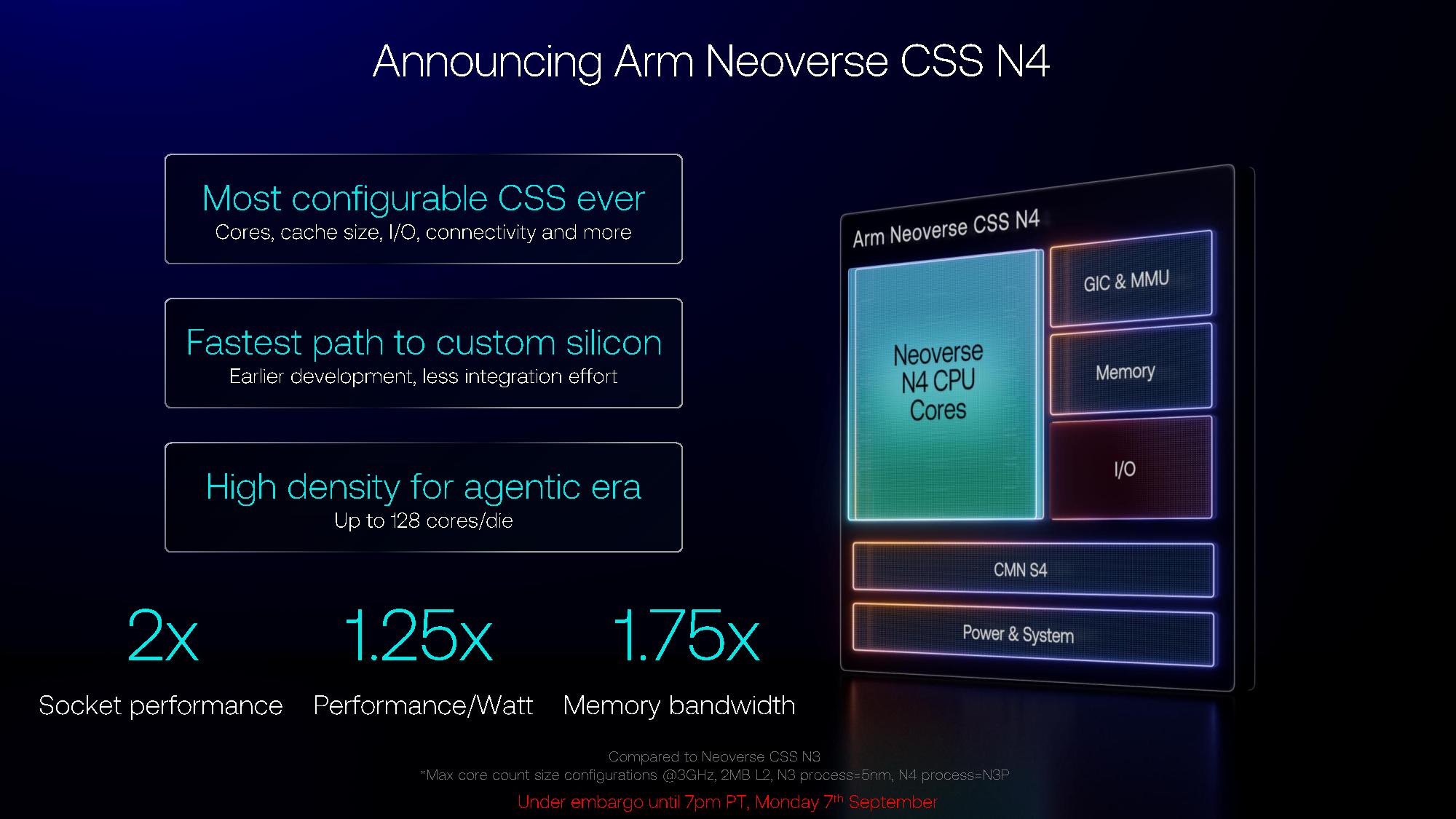
Arm is bringing its next-gen Neoverse CSS N4 platforms to the cloud, sporting up to 128 cores per die, built on TSMC’s N3P process. Arm’s Compute Subsystem, or CSS, is a semi-custom program that allows customers to design a chip based on Arm’s IP, configuring components like core count, cache size, I/O, and connectivity to fit their specific needs. It’s the same platform we’ve seen at work everywhere from CPUs at Azure and Google Cloud to DPUs at Nvidia and Intel.
Arm says Neoverse CSS N4 supports between eight and 128 Neoverse N4 cores, running up to 3.8 GHz. Presumably, the clocks drop as the core count rises; Arm didn’t clarify the maximum clocks for each possible configuration. At a system level, Neoverse CSS N4 can scale beyond 128 cores, with support for multi-chiplet and multi-socket designs, and with support for UCIe through chip-to-chip interconnects, as well as “partner-specific PNYs.”
The platform supports either DDR5 or LPDDR6, and features up to 256 MB of L3 cache per die. For local cache, Arm includes up to 2 MB of L2 per core, as well as 64 KB of L1 instruction cache and 64 KB of L1 data cache per core. For I/O, Arm supports up to 128 lanes of PCIe 7/6 and CXL 4.0.
It’s a significant upgrade over the Neoverse CSS N2 platform, which topped out at just 64 cores, 1 MB of L2 cache per core, and 64 MB of L3 cache, paired with either DDR5 or LPDDR5 and 64 PCIe 5.0/CXL lanes.
(Image credit: Arm)
With 128 cores running at 3GHz and 2MB of L2 cache per core, Arm says Neoverse CSS N4 delivers twice the socket performance of Neoverse N3, 1.25x performance per watt, and 1.75x the memory bandwidth.
Arm’s N-series cores are optimized for performance per watt, while its V-series cores are targeting maximum performance. For instance, Arm used the Neoverse CSS V3 building blocks for its own AGI CPU, and Nvidia used Neoverse V2 for its last-gen Grace CPU (the Vera CPU uses a custom core). AWS has also used Neoverse V-series cores for its own Graviton chips, as does Google Cloud for Axion.
N-series cores aren’t usually deployed in high-performance CPUs. Rather, they fit into less-performant accelerators, such as Intel’s IPU Adapter E2100, which is built on Neoverse N1 cores. We’ve also seen it deployed in less-demanding, cloud-based workloads, such as through Microsoft’s Azure Cobalt 100, which is built on Neoverse N2. Cobalt 200 moved onto Neoverse V3.
We don’t know much about the Neoverse N4 cores, codenamed Dionysus. Arm’s 2024 roadmap indicated we’ll see Arm Neoverse CSS V4, as well, codenamed Vega.
Unlike a traditional announcement from Intel, AMD, or the various partners that build on Arm, we won’t see Neoverse N4 cores in the wild for a while. The announcement Arm is making is for those who are building on the CSS platform, leveraging Arm’s validated building blocks to create semi-custom silicon quickly. Arm has yet to announce any partners, though traditionally, only a few large CSS contracts are needed.
Additional Arm AGI CPU deployments
(Image credit: Arm)
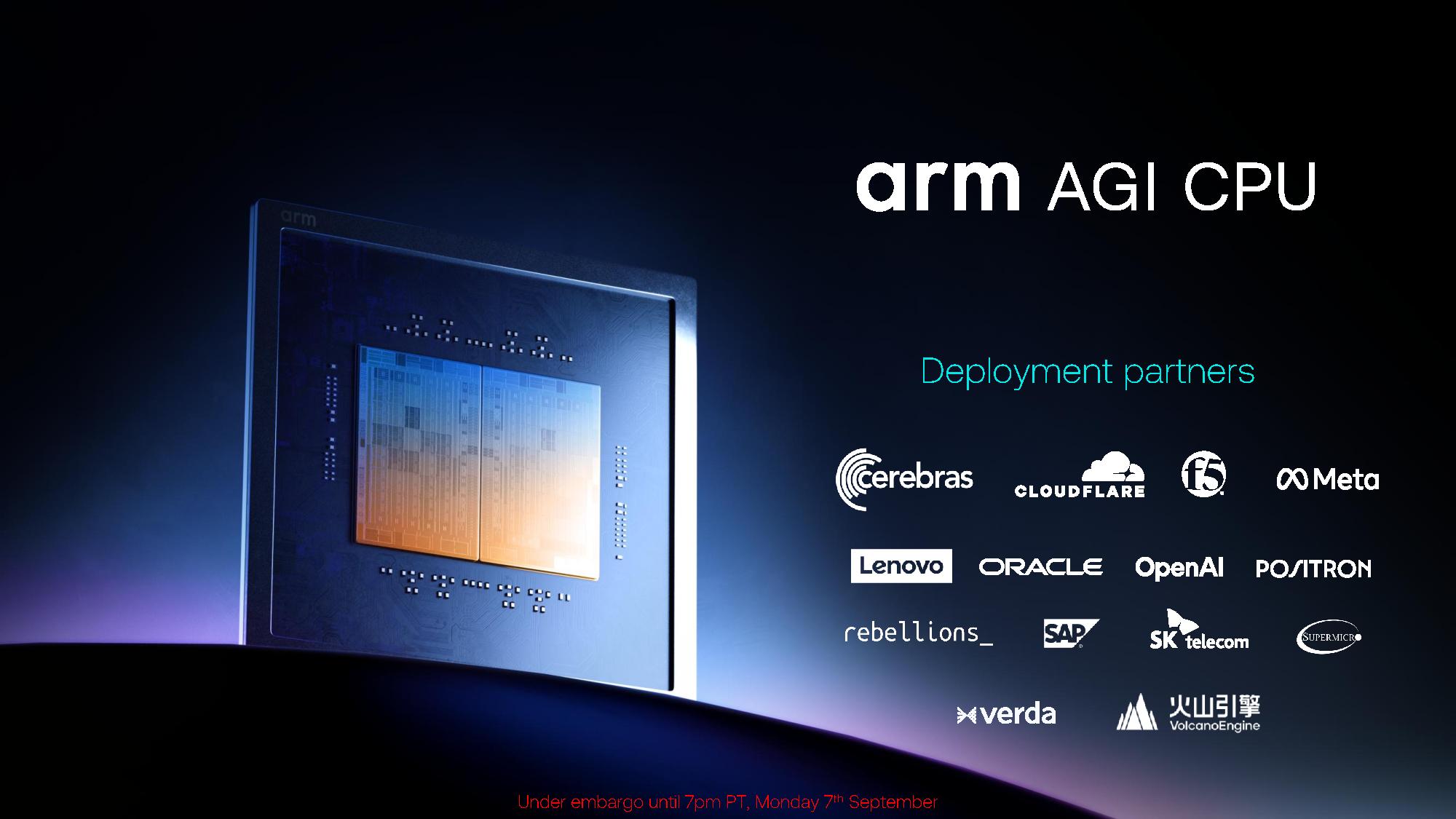
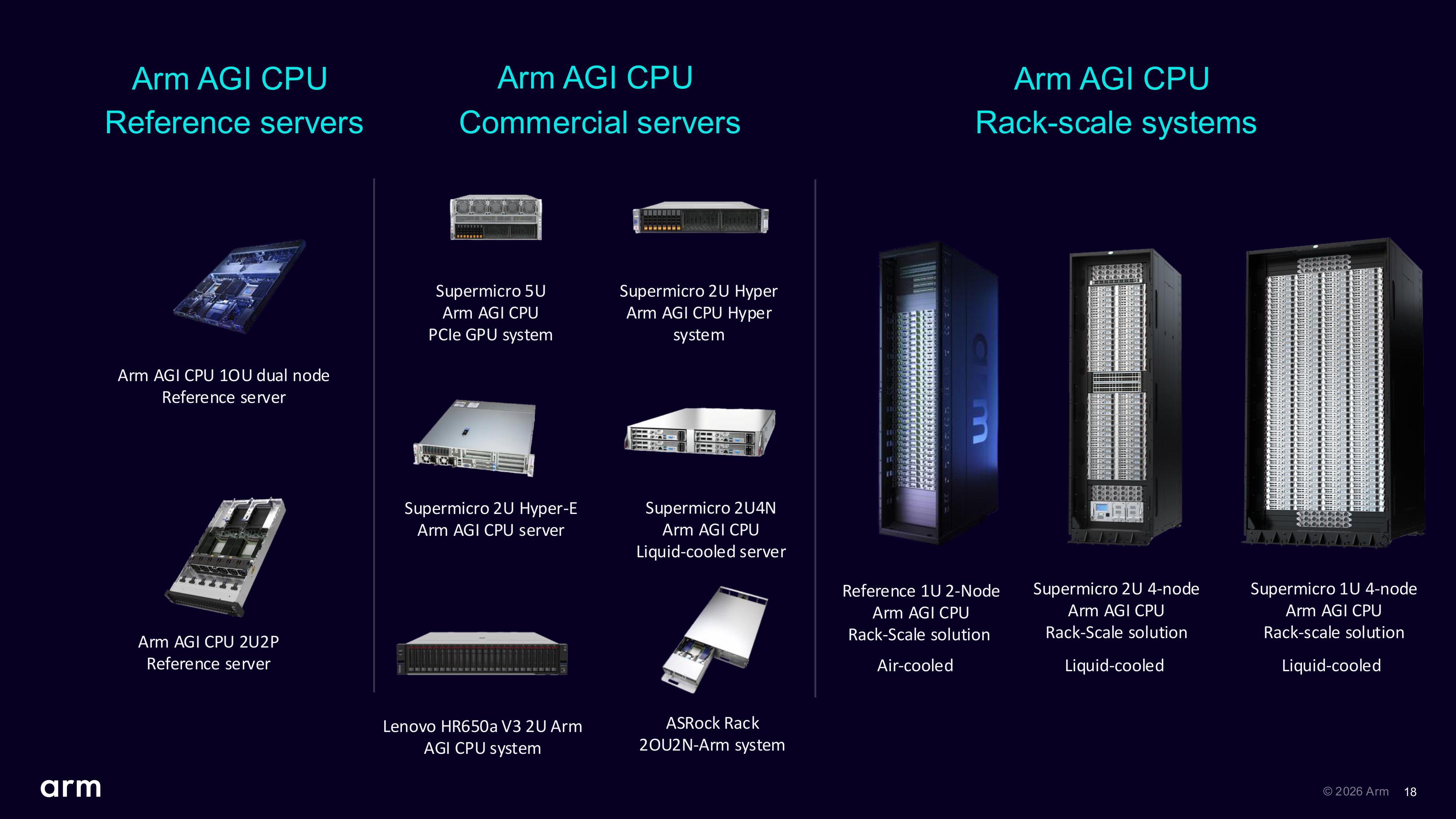
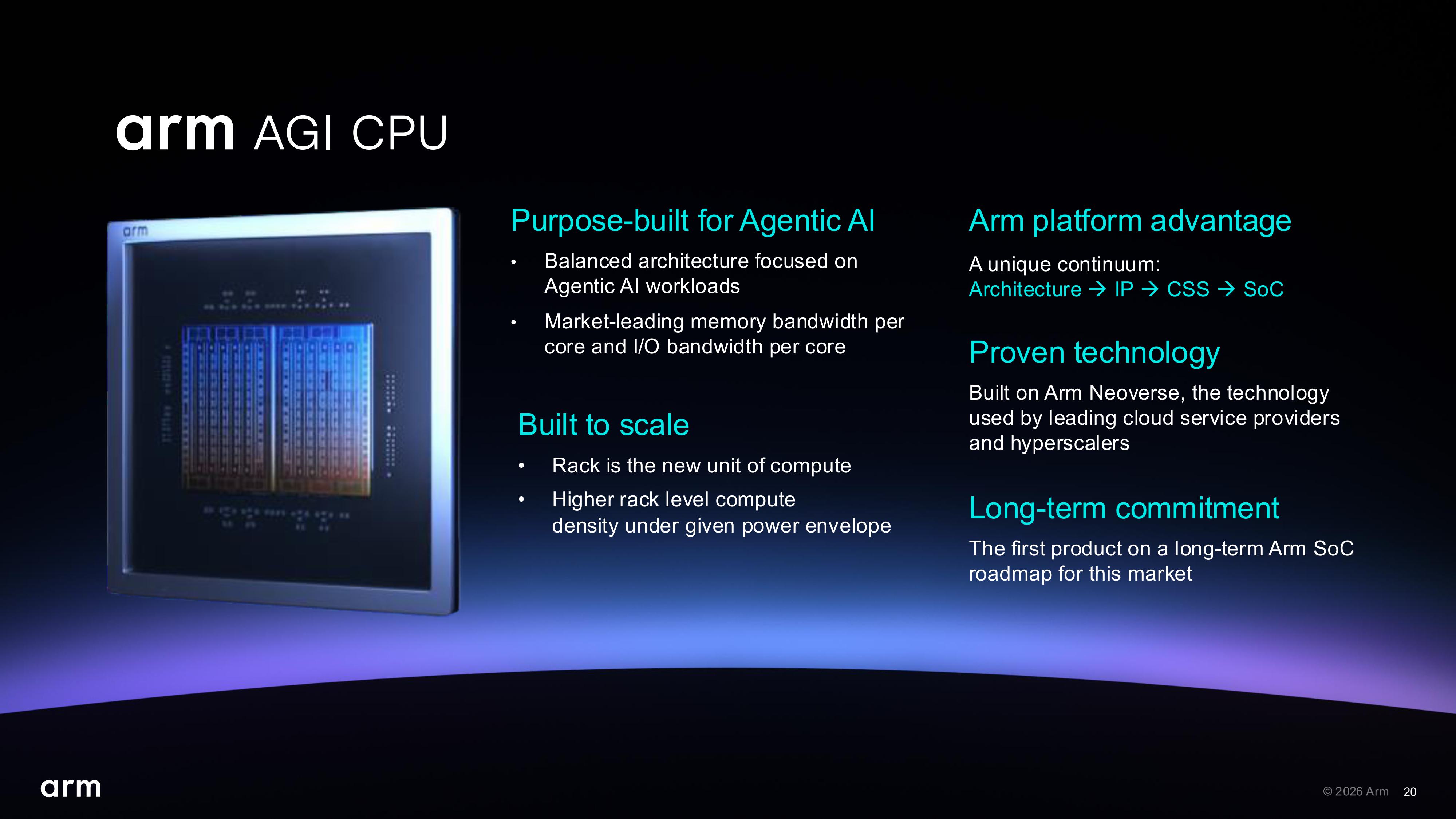
Alongside the announcement of Arm Neoverse CSS N4, the company revealed additional deployments of its own AGI chip, which is built with Neoverse V3 cores. The company revealed that Oracle and ByteDance will deploy AGI chips, alongside previously announced deployments at Meta, Lenovo, SAP, OpenAI, Cloudflare, and others.
Although Arm has talked a lot about AGI, including a deep dive into the chip’s architecture at Hot Chips, we’ve yet to see real-world performance numbers. That’s not uncommon, especially among more recent Arm-based chips. For instance, we only have gen-on-gen comparisons for Microsoft’s Azure Cobalt 200 and AWS’ Graviton5. Arm has vaguely referenced performance by saying AGI offers “more than 2x the performance per rack compared to the latest x86 systems,” though those claims are based on internal estimates, not real benchmarks.
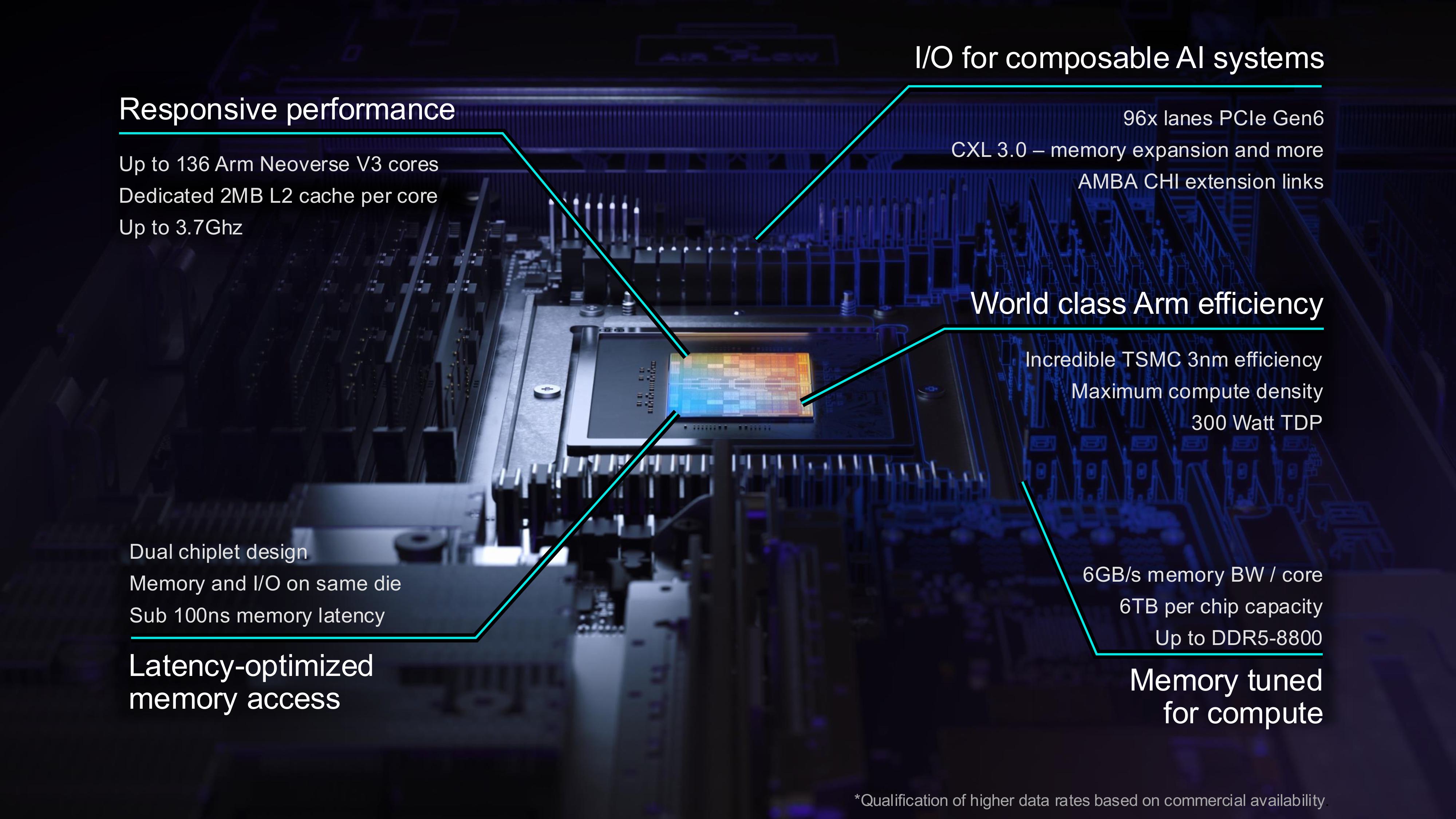
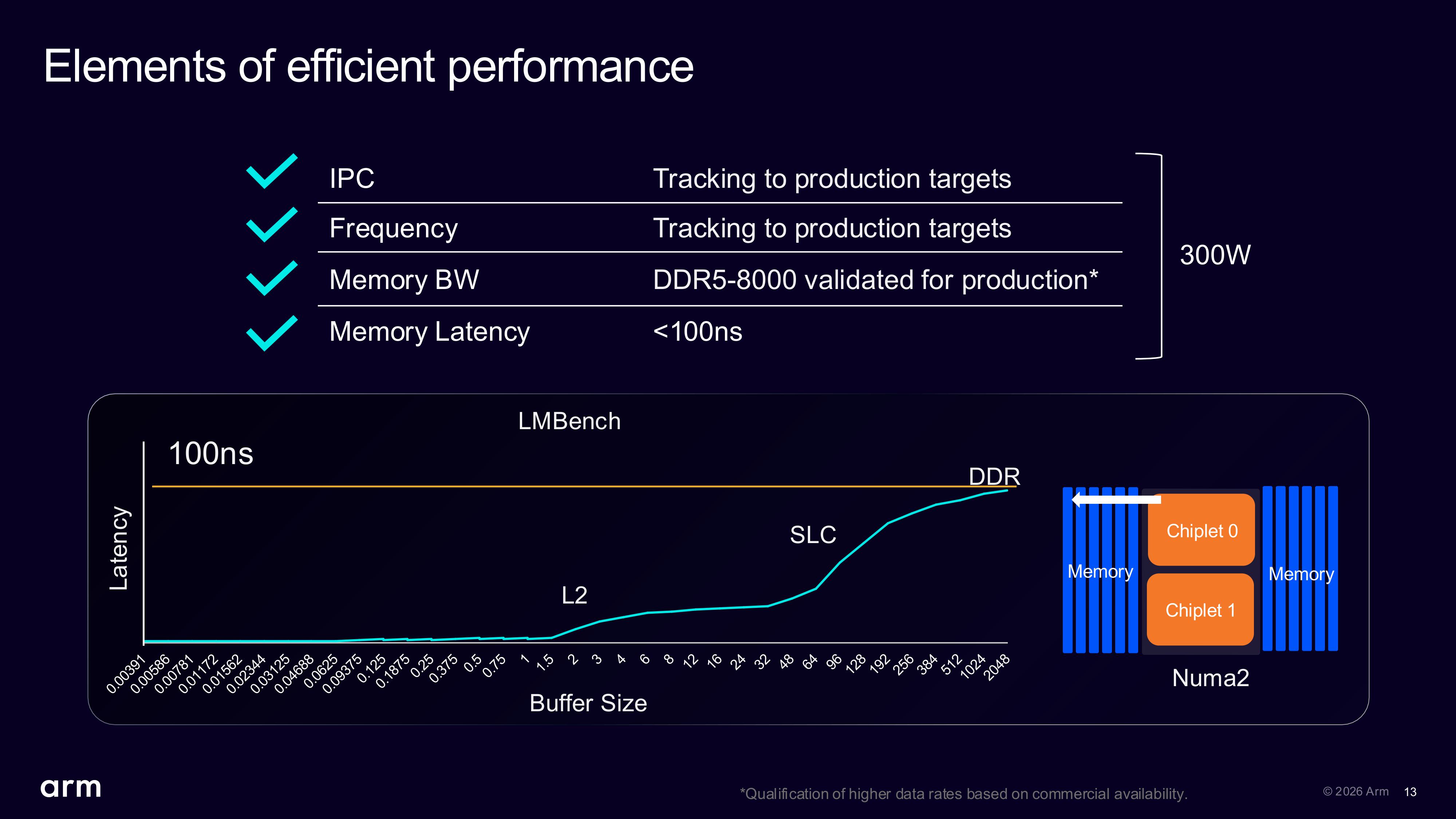
AGI is a dual-die CPU with up to 136 Neoverse V3 cores and up to 272 MB of L3 cache that can clock up to 3.7 GHz. It has the specs to match any high-end x86 design currently on the market, built on a 3nm node and packing up to 6TB of memory capacity per chip, running at up to DDR5-8800. Perhaps the biggest difference compared to AMD and Intel was Arm’s decision to include the memory and I/O on the same die as compute, which it says leads to sub-100ns memory latency.
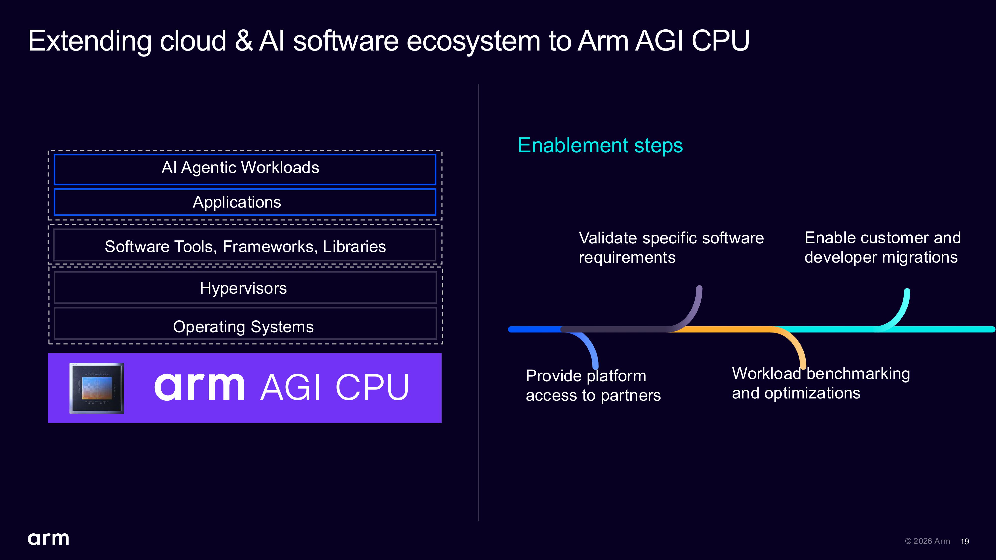
It’s Arm’s first attempt at its own production silicon, though it’s also been positioned so far as a vehicle for the broader applications of Arm in the data center. Microsoft, Nvidia, Meta, Google Cloud, and others build custom chips based on Arm IP, which still seems to be the primary goal, even with AGI in the mix.
AMD is no stranger to refreshing its older CPU families with new SKUs, especially since the consumer hardware market for new products is currently in a slump. Ryzen 7000 is a relatively new lineup for the company, but it seems like it might be the latest recipient of this strategy. Leaker Roland Quandt is reporting that a Ryzen 5 7500 non-F is coming soon with specs identical to the 7500F, but at double the price for some reason.
AMD Ryzen 5 7500 (no F, no X3D, no nothing) incoming.AM5 socket3,7 GHz, up to 5,0 GHz boost6C/12T38MB cache in total65W TDP~230 Euro
As the post above clarifies, this is a bog-standard chip with no 3D V-Cache or anything extra. Actually, that's not entirely factual, as ditching the "F" moniker means the processor is gaining integrated graphics. However, given what we see on the Ryzen 5 7600, this iGPU will comprise only two small RDNA 2 CUs. That's enough for a display output and everyday tasks, but don't expect to be gaming on this thing.
The rest of the specs remain unchanged from the Ryzen 5 7500F. Its rumored non-F counterpart is also a six-core, twelve-thread CPU with a 3.7 GHz base clock and 5.0 GHz boost clock. You'll get 38MB of combined cache, likely a 32MB L3 + 6MB L2 split, along with a 65W TDP. All those match the 7500F, with the only glaring difference being the price — the Ryzen 5 7500 is supposed to somehow retail for 230 Euros, or $267 freedom units.
For context, the Ryzen 5 7500F launched at $179 three years ago but quickly came down in price and can be had for just $116 right now. Even in Germany, it costs 105 Euros at the moment, which translates to $122. Moreover, for the $250+ price rumored for the 7500 non-F, you can instead get the much more powerful Ryzen 5 9600X along with a whole B850 motherboard on Newegg as we speak. You can even find the 7600X3D for less than $250 on Amazon right now.
The only way one could try to justify this pricing is by arguing that the 7500 non-F comes with a box and cooler, unlike the 7500F, which is a tray-only package. Then again, these comparisons are based on current pricing, and we know how much of a mirage that can be during the component crisis. Price hikes for CPUs are not a rarity anymore, and since we don't have a rumored launch window for the 7500 non-F, it could coincide with one.
That's just speculation, though; take everything you just read with a grain of salt. The reason the rumored price is in Euros to begin with is that the leaker is based in Germany. We don't even know if this chip will receive a global launch.
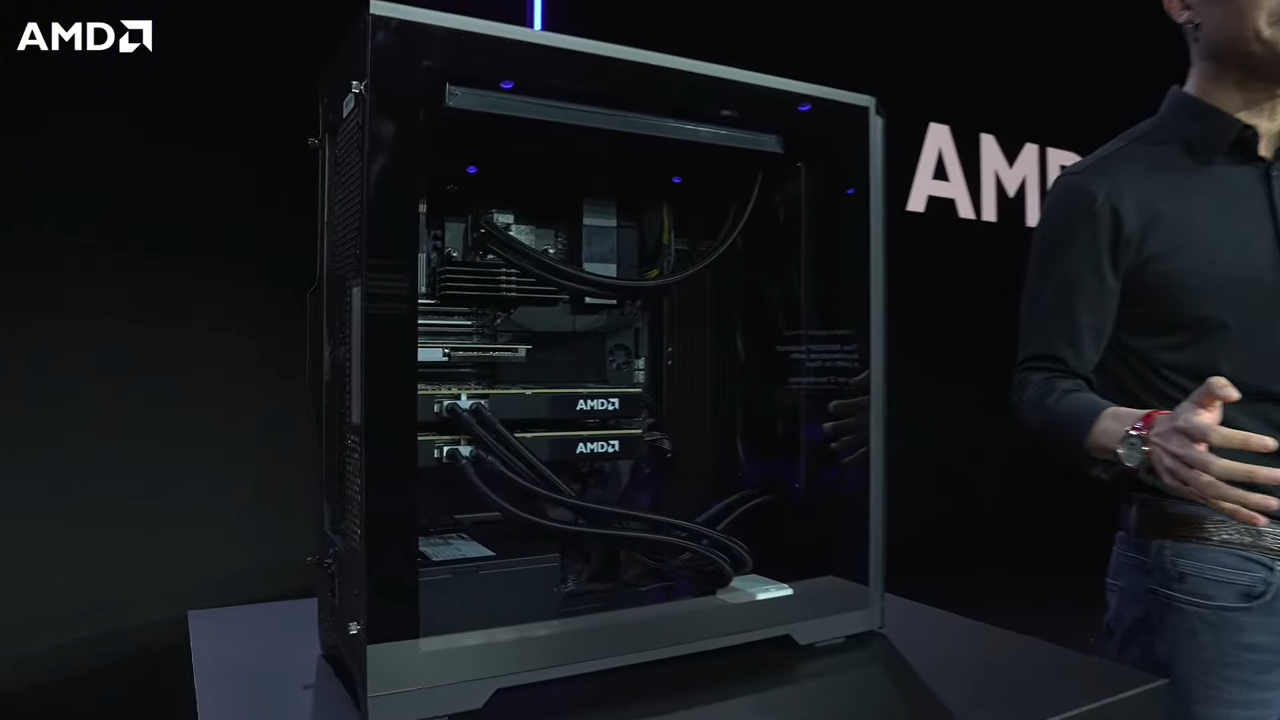
AMD announced what it calls "the most powerful workstation in the world" at IFA 2026, dubbed the Threadripper Halo Station. The machine includes a Threadripper Pro 9995WX with 96 Zen 5 cores, dual liquid-cooled Instinct MI350P accelerators "with a path to four," 2TB of DDR5, and 288GB of HBM3E with up to 576GB supported. AMD claims the workstation is capable of running trillion-parameter models.
Taking all of the components together, the street price should come out to over $100,000 with just the core components: memory, CPU, and dual GPUs. Configured higher, and with supporting storage, power, and cooling, the workstation could very easily climb over $150,000.
It's essentially a server tray reconfigured into a tower, with an EPYC host replaced with a 96-core Threadripper. AMD didn't share many details about the machine outside of the specs, though it appears to be a system design that AMD's OEM partners will ultimately build and ship. AMD has yet to announce any partners supporting the machine.
The Threadripper Pro 9995WX at the heart of the machine is a 96-core, 192-thread Zen 5 chip that can boost up to 5.4 GHz. It ships with 384 MB of L3 cache and has a TDP of 350W. It's hard to find Threadripper Pro standalone chips in general, but the 9995WX clocks in at around $11,000 to $12,000.
CPU Host
Threadripper Pro 9995WX, 96 cores, 5.4 GHz boost
GPU
2x Instinct MI350P
System memory
2TB DDR5
Cooling
Liquid-cooled CPU and GPUs
GPU memory
144GB HBM3E per accelerator, up to 576 HBM3E
CPU TDP
350W
GPU TBP
600W (per accelerator)
The MI350P accelerators come with 128 CDNA 4 compute units built on TSMC N3. Each accelerator packs 144GB of HBM3E memory, giving the system 288GB of HBM3E. AMD says there's a "path to four," opening up the possibility of two more accelerators bringing 576GB of HBM3E to the system. You'll need plenty of power to feed the GPUs, as each accelerator is rated for up to 600W.
Although AMD says it can support up to four accelerators, the workstation shown off at IFA only has room for two, both of which are liquid-cooled, alongside the Threadripper host. AMD doesn't sell MI350P accelerators on their own in traditional consumer channels, but the estimated price is somewhere around $20,000 per accelerator.
At a system level, the Threadripper Halo Station includes 2TB of DDR5 memory, which is the maximum capacity supported across the eight-channel memory configuration of the Threadripper Pro 9995WX. AMD supports up to DDR5-6400 on the Threadripper, though it made no mention of speed during its IFA presentation. Regardless of speed, 2TB of DDR5 costs about $50,000 right now.
AMD has yet to set a price or release date for the Threadripper Halo Station, though we'll likely hear more about the design from AMD's partners in the near future. An extremely expensive workstation isn't out of the question. The Lenovo ThinkStation P8, for instance, which uses Threadripper Pro CPUs as a host, clocks in at $334,463 right now, maxed out with 2TB of DDR5 and dual Blackwell accelerators.
Intel's upcoming Core Ultra 400-series 'Nova Lake-S' CPU platform promises to be the company's biggest desktop launch in years, with range-topping processor offering up to 52 cores and gaming processors featuring up to 288 MB of bLLC cache, at least according to the rumor mill. Intel is reportedly on track to start mass production of its Nova Lake-S CPUs in the fourth quarter of 2026, according to a slide published by @wxnod. However, only the 28-core version will launch in the first quarter of 2027, with the 52-core model arriving later in the year, as we covered out of this year's Computex.
When initial leaks and roadmap disclosures about Intel's Nova Lake-S surfaced across 2025, the projected production schedule placed mass production in Q4 2026, so the new slide confirms that plan. Meanwhile, the actual CPU roll-out will be somewhat different to what Intel is used to as the company only intends to release unlocked 28-core SKU (or SKUs) in Q1 2027 and push the release of flagship models allegedly using two compute tiles featuring up to 52 cores to sometimes later in 2027. Some rumors pointing to a timeframe between late May and September, 2027. Normally, Intel launches flagship and unlocked models first. However, reports suggest the 52-core model will fit in a different class above a typical flagship, primarily targeting the HEDT crowd.
The slide revealed by the blogger does not look like an official Intel roadmap or an Intel presentation slide. A more plausible explanation is that the slide comes from a motherboard maker's presentation (or one of Intel's OEM partners), which compiled information the manufacturer got from Intel, which means that while it is most likely accurate, it is not final.
Intel's Core Ultra 400-series 'Nova Lake-S' CPUs will reportedly use up to 16 all-new high-performance Coyote Cove cores with 16MB of L2 cache, up to 32 energy-efficient Arctic Wolf cores, and up to four low-power Arctic Wolf cores, according to various leaks and the slide published by @wxnod. Even though each pair of Coyote Cove cores will reportedly share a 2 MB L2 cache, which will inevitably affect single-thread performance, Intel has an ace up its sleeve in the form of bLLC (big Last Level Cache), which will apparently scale to 288 MB to offer unbeatable performance in memory bandwidth-hungry applications, if media reports are correct. bLCC is apparently Intel's plan to fight back against AMD's X3D CPUs, which top the charts among the best CPUs for gaming.
The highest-end Core Ultra 9 400-series processors are expected to pack up to 52 cores using two compute tiles, whereas Core Ultra 7 400-series models are projected to feature up to 44 cores using two compute tiles, though exact configurations are currently unknown. Meanwhile, CPUs with two compute chiplets will reportedly consume up to 474W of power and will require motherboards featuring three 12V EPS power plugs.
On the I/O side of matters Intel's Nova Lake processors will reportedly feature a dual-channel DDR5 memory subsystem supporting up to DDR5-8000 modules as well as provide up to 24 PCIe 5.0 lanes directly from the CPU, including 16 lanes for graphics that can be split into two x8 or four x4 connections, plus two x4 links for SSDs.
Intel's new Core Ultra 400-series 'Nova Lake-S' processors for desktops will require Intel's new 900-series chipsets as well as will use an LGA1954 socket, according to leaks. Intel reportedly intends to keep LGA1954 around for a longer time than it usually does with its sockets, ensuring an upgrade path for years to come. We've already seen Z990 motherboards sporting the LGA1954 socket in the flesh.
Speaking of years to come, the slide lists Razor Lake and Hammer Lake processors that will succeed Nova Lake-S sometime after the fourth quarter of 2027. The slide does not provide technical details about either family, and we can only wonder whether Razor Lake corresponds to Core Ultra 500-series and Hammer Lake belongs to the Core Ultra 600-series, or both will be a part of one CPU family.
Onimusha: Way of the Sword closes out an incredible year for Capcom, following hot on the heels of both Resident Evil Requiemand Pragmata earlier in the year. Like those titles, the game is built on Capcom’s proprietary RE Engine, which has proven to be a remarkably scalable engine that can accommodate a wide range of hardware. We put some of the best CPUs for gaming through the game’s free benchmark to see how it scales on the CPU.
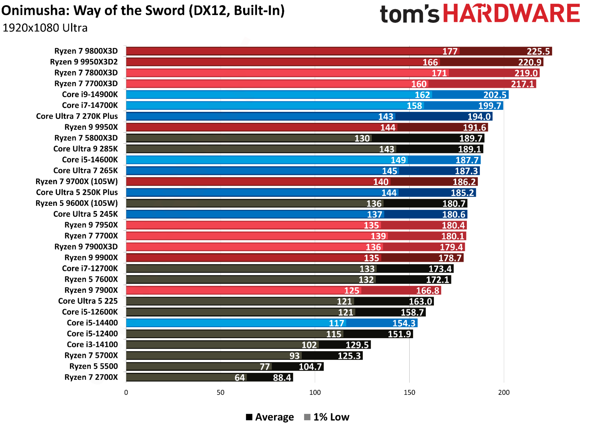
RE Engine is heavier on the GPU than the CPU, but still, we saw scaling across the 31 CPUs we tested, ranging from new releases like the Core Ultra 7 270K Plus, reaching back to relics of the past decade like the Ryzen 7 2700X. Largely, performance falls as you’d expect, but there were a few odd results that showed up in our testing, namely for AMD’s newer 12-core Ryzen 9 models, which struggle to keep pace in this game.
Regardless, the game runs well on a wide range of hardware. Even with the RTX 5090 Founder’s Edition we tested with the Ryzen 7 2700X, completely binding performance to the CPU, we neared 90 FPS at 1080p with Ultra settings and no ray tracing.
This is a cursory look at Onimusha: Way of the Sword using the in-game benchmark available (we’ll go over how we tested a bit later). As usual, performance will vary from scene to scene, and we’ve yet to reach the latest areas of the game, which may have an adverse impact on performance (though we don’t expect one). We are looking at how CPUs scale in the game more so than the raw frame rate of any individual chip.
CPU scaling in Onimusha: Way of the Sword
The Onimusha: Way of the Sword benchmark is about five minutes long, primarily consisting of two in-engine cutscenes rendered in real time. The back half of the benchmark features gameplay, which shows considerably lower performance and taxes the CPU far more than the cutscenes. We chose to benchmark during the gameplay section, naturally.
We tested with the Ultra preset without ray tracing enabled. We didn’t use DLSS or FSR, either. As usual, we tested at 1080p with the RTX 5090 Founder’s Edition to isolate CPU performance as much as possible. We’ll go deeper into the specific system configuration for each platform later in this article if you’re interested. For each CPU, we ran the benchmark three times and took the median result, discarding and rerunning any outliers.
(Image credit: Tom's Hardware)
Out of the 31 CPUs we tested, the obvious ones to call out first are AMD’s 12-core Ryzen 9 offerings, because they perform poorly in this game. The Ryzen 9 7900X is actually 3% slower than the Ryzen 5 7600X, and similarly, the Ryzen 9 9900X is 1% behind the Ryzen 5 9600X. There’s clearly some issue with the 12-core parts, specifically, that doesn’t show up in the single-CCD Ryzen CPUs, nor the full, 16-core, dual-CCD models.
Great evidence of that is the Ryzen 9 7900X3D, which I only chose to run to see if 3D V-Cache would be able to overcome the 12-core penalty. It wasn’t able to. Every other X3D chip we tested sits at the top of the charts, while the Ryzen 9 7900X3D ended up in lockstep with the Ryzen 7 7700X. It’s possible this is a performance issue that either Capcom will address through a patch, or AMD through a firmware update. Regardless, the 12-core Ryzen 9 performance in this game is rough right now.
Elsewhere, things are great. X3D chips top the charts, though with less of a margin than we see in other titles, and virtually no margin in comparison to one another. The Ryzen 7 7700X3D is 7.2% ahead of the Core i9-14900K, Intel’s strongest CPU in this game, while the Ryzen 7 9800X3D extends that lead up to 11.3%. We didn’t have time to benchmark the Ryzen 7 9850X3D, though based on the negligible performance gap between the 7700X3D and 7800X3D, don’t expect any miracles.
The Ryzen 7 5800X3D doesn’t reach the heights of its DDR5-equipped siblings, falling 13.4% behind the Ryzen 7 7800X3D. It still puts on an excellent showing considering its peers, sitting among the Core Ultra 9 285K and Ryzen 9 9950X. Even four years down the road, the Ryzen 7 5800X3D delivers performance on the level of current-gen flagships, at least in this title.
In Intel’s camp, the Core i9-14900K remains the fastest chip in Onimusha, at least when equipped with DDR5 (read our DDR4 vs DDR5 Raptor Lake comparison to see the difference in performance). Unfortunately for Team Blue, even the Core i7-14700K is 2.9% faster than Intel’s latest Core Ultra 7 270K Plus in this game. Intel doesn’t have support for Onimusha with iBOT, nor any RE Engine titles, suggesting that the performance you see here is the cap for Arrow Lake Refresh. Hopefully that changes with Intel’s impending Nova Lake.
Although Arrow Lake and AL Refresh don’t scale as high as the 14th-Gen offerings, performance is still solid competitively. The Core Ultra 5 245K is in lockstep with the Ryzen 5 9600X, as expected, while the lowly Core Ultra 5 225 is nipping at the heels of the Ryzen 5 7600X.
(Image credit: Tom's Hardware)
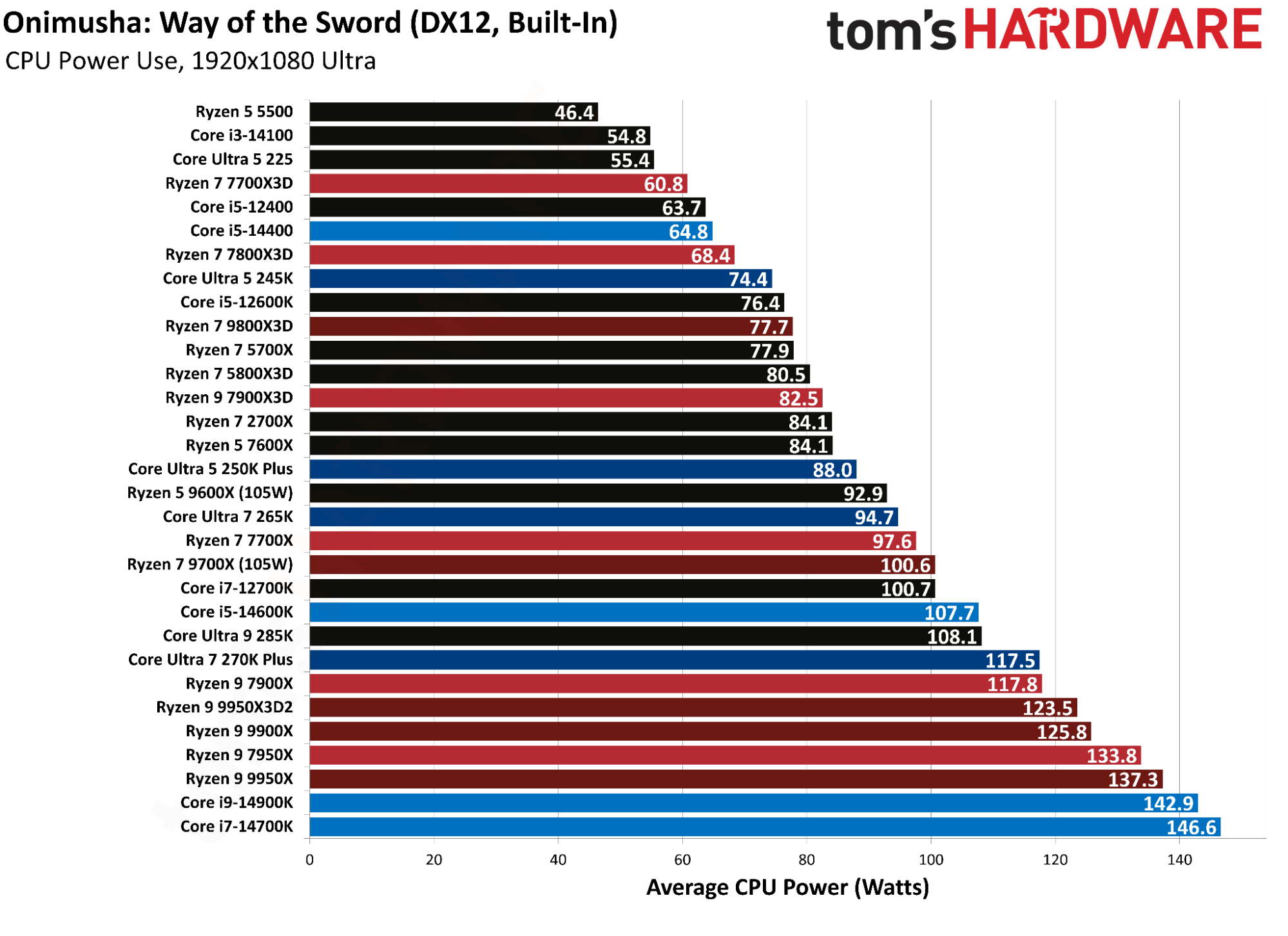
Flipping over to power, X3D chips remain well under 100W, short of the dual-CCD, dual-cache Ryzen 9 9950X3D2. Intel’s Raptor Lake Refresh chips unsurprisingly had the highest power usage out of our test pool, with the Core i7-14700K actually drawing a bit more power than the Core i9-14900K. Although we ran the test multiple times, we took the median result for average frame rate, which can sometimes push neighboring figures out of sorts when looking at other metrics. We don’t want to mix power results from one run and performance from another.
(Image credit: Tom's Hardware)
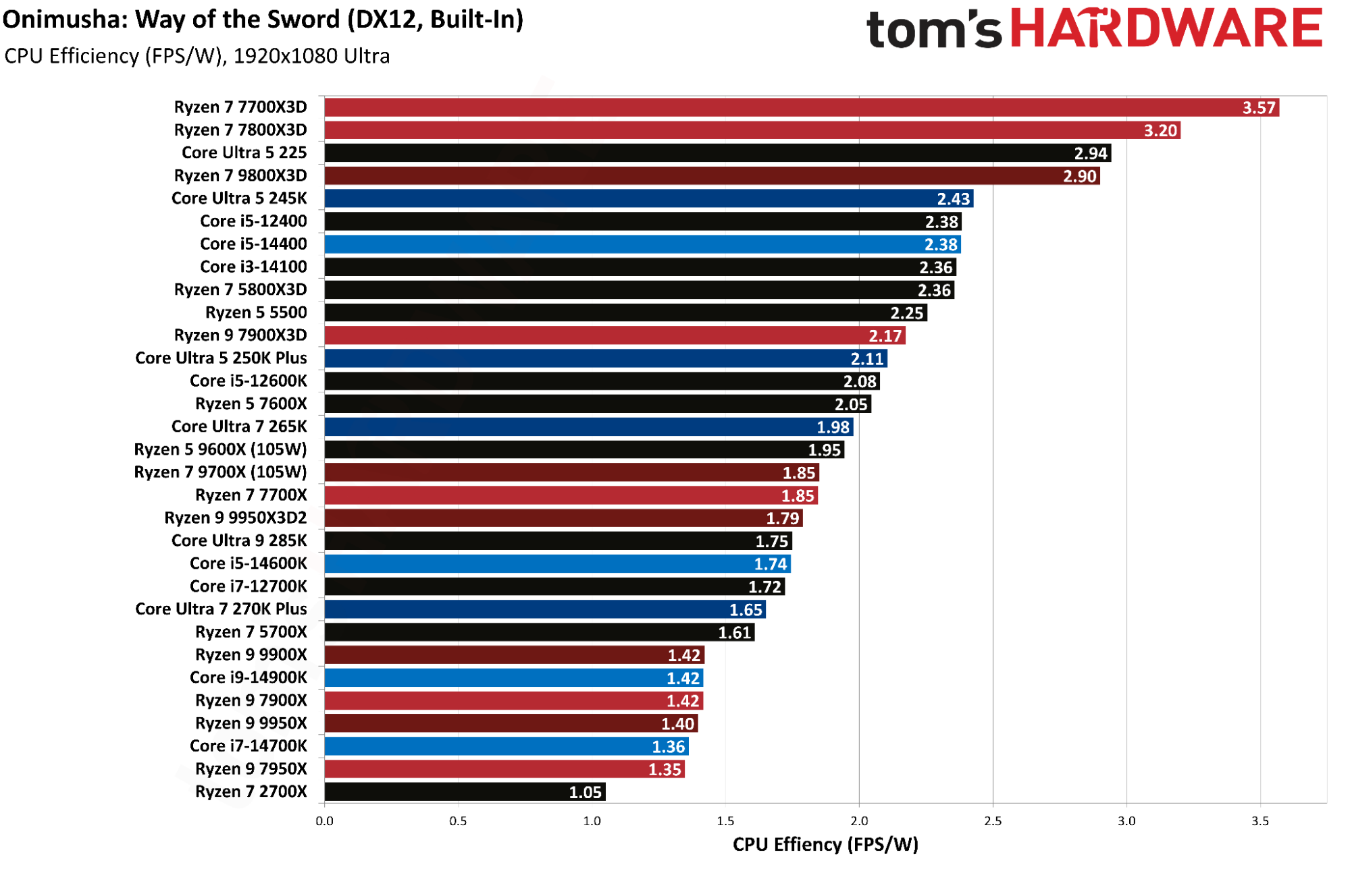
Looking directly at efficiency, the Ryzen 7 7700X3D was the most efficient chip in our testing, offering up just over 3.5 frames per watt consumed. The Ryzen 7 7800X3D barely offered a performance benefit over the 7700X3D, so its efficiency suffers as a result. Even the Ryzen 7 9800X3D falls below the 3-frames-per-watt mark.
(Image credit: Tom's Hardware)
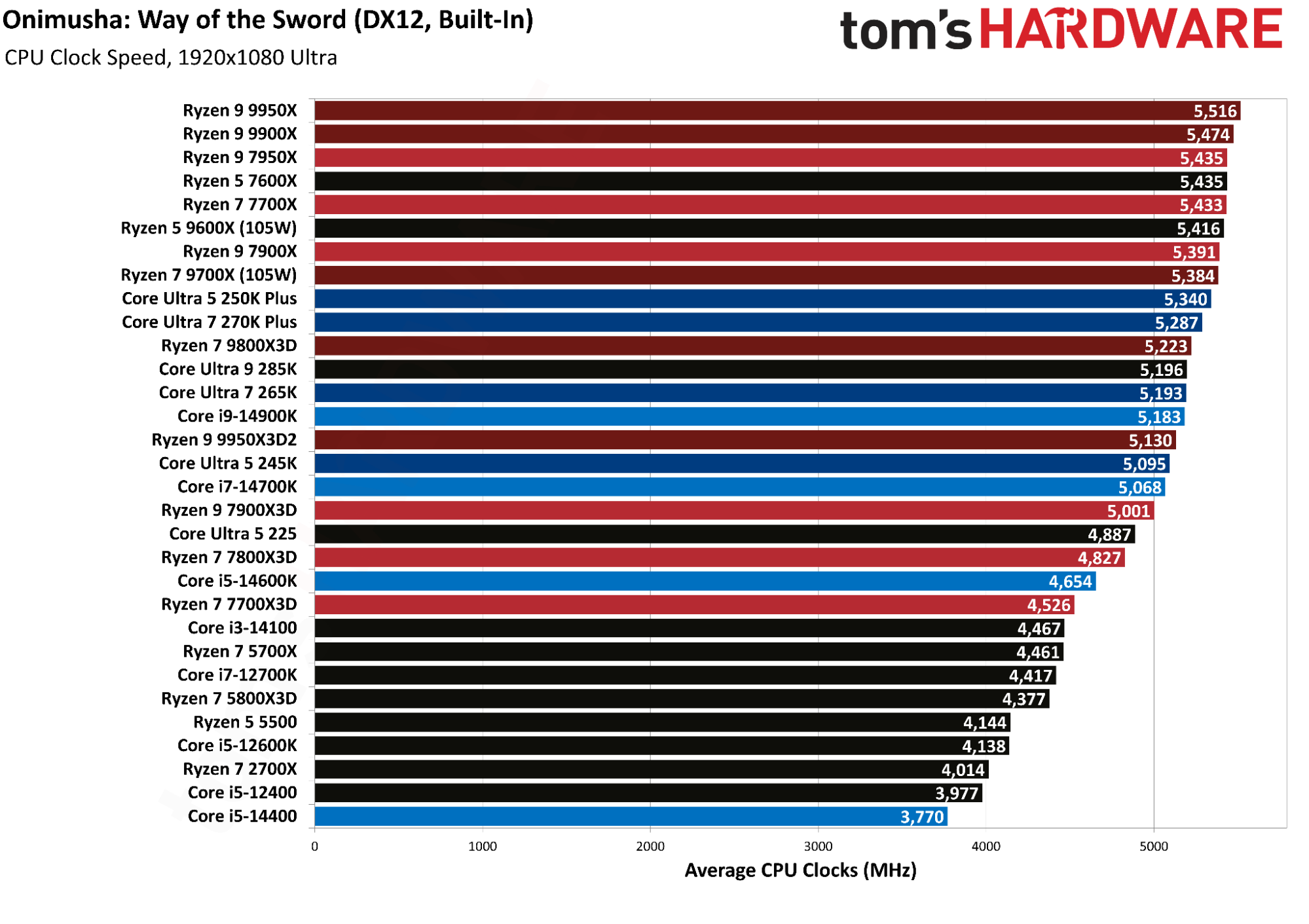
Finally, clock speed doesn’t offer a lot of surprises. The more efficient CPUs like the Ryzen 7 7800X3D ran right up against their maximum boost clock on average, while flagships that push single-core speed to the limit like the Ryzen 9 9950X and Core i9-14900K fall below their maximum boosts. Clocks don’t translate into performance here, though looking at this chart combined with our averages provides some insight into how threaded Onimusha is.
It’s lightly threaded, like the vast majority of games, though there’s a clear bump in performance beyond four cores. Combined with lower maximum boost clocks on high-core-count flagships, all-core clocks are certainly more relevant here than single-core boosts. Then again, clock speed isn’t a major factor here, regardless.
How we tested Onimusha: Way of the Sword
We used our normal test bench used for CPU reviews, as well as our CPU benchmark hierarchy testing. The hardware doesn’t change, short of the CPU and, when necessary, the motherboard and memory. We also use a frozen OS image, meaning we’re running the same versions of the same software with all the same dependencies for each test pass.
The GPU we used is the RTX 5090 Founder’s Edition, as our goal when looking at CPU scaling is to isolate the CPU’s performance as much as reasonably possible. Naturally, running a game at a low resolution like 720p and turning down all of the graphics options will put even more pressure on the CPU, but that pushes beyond isolating the performance of one component in a relatively realistic testing environment.
Although the hardware is consistent, there are BIOS tweaks we make depending on the platform. As a broad rule, anything we enable that improves performance is covered under warranty. If performance-enhancing features void the warranty, we leave them disabled. That includes AMD’s Precision Boost Overdrive and Intel’s Extreme power profile. We also don’t enable any motherboard-specific performance enhancements, such as tweaked XMP/EXPO profiles or X3D enhancements.
For this test pool, there are some features still covered by the warranty that improve performance. In Intel’s camp, we tested with Core Ultra 200S Boost enabled on all supported Arrow Lake CPUs (the 225 doesn’t support the feature). Similarly, the Ryzen 5 9600X and Ryzen 7 9700X run at a 65W TDP out of the box, but an optional, warrantied 105W TDP mode is available. We tested with that mode enabled.
We also disabled Virtualization-Based Security (VBS), as it can adversely affect gaming performance.
Intel notified its employees last week that it would no longer title its top scientists, researchers, and developers as 'Fellows,' but will call them 'distinguished engineers,' a change that will not affect their compensation but which means a lot more than a simple formality. The new designation reflects the company's new 'standard of technical leadership' that combines deep expertise with strategic vision and 'measurable tactical progress,' reports OregonLive.
Under the new hierarchy, Fellows become Distinguished Engineers, while Senior Fellows become Senior Distinguished Engineers. Intel CTO Pushkar Ranade told employees that the move represents more than a simple renaming and establishes a new standard for technical leadership.
"The future of Intel will be determined by leaders who combine deep domain expertise with outstanding problem-solving ability, creative innovation with disciplined execution, and an expansive and strategic vision with measurable tactical progress," the Intel CTO reportedly wrote.
Interestingly, despite the fact that at least a dozen semiconductor companies — including AMD, ASML, Applied Materials, Arm, Broadcom, IBM, Nvidia, Micron, Texas Instruments, Qualcomm, and TSMC — have Fellows, Ranade told Intel employees that the new titles are more consistent with terminology used elsewhere in the technology industry. While Apple, Google, IBM, and Microsoft have Distinguished Engineers, at Google, IBM, and Microsoft, Fellows are above Distinguished Engineers.
Intel established the Fellow title in 1980 to recognize employees with a sustained record of exceptional technical accomplishments. The designation had deliberately academic roots because scientific societies and then engineering organizations have long used 'Fellow' for distinguished members, for example, the Fellow of the Royal Society (FRS) or IEEE Fellow. So, by the time semiconductor companies, such as IBM, TI, or Intel, were developing formal technical career ladders, Fellow already carried a very specific implication: an engineer recognized by their peers as one of the leading authorities in the field.
Across semiconductor companies, the Fellow rank typically carries compensation, resources, and influence equivalent to a vice president (VP) or senior vice president (SVP), so that top architects and device physicists can shape company strategy without moving into people management (yet, Fellows did not work alone for obvious reasons). It is unclear whether Distinguished Engineers will now have similar resources and influence as Intel's VPs and SVPs that report to the CEO. Furthermore, at Intel, the Fellow (or senior Fellow) title reflected Intel's position as a semiconductor research powerhouse as well as its emphasis on long-term technology development.
The most notable people to hold the Intel Fellow rank title include distinguished specialists in microprocessor architecture, process scaling, high-speed interconnects, and silicon physics, including Marcian 'Ted' Hoff (the inventor of the Intel 4004 processor), Justin Rattner (for his work on massively parallel supercomputers), Mark Bohr (for leading Intel process technology development and fundamental work on things like strained silicon, hafnium, high-K metal gate, FinFET, etc.), Yan Borodovsky (for leading development and adoption of optical lithography extensions, immersion 193nm ArF lithography, and multi-patterning, just to name a few), and Ajay Bhatt (for leading development of USB, AGP, and PCIe). Perhaps the most unexpected Intel Fellow is Boris Babayan, who is primarily known as the father of Soviet supercomputing and the creator of the Elbrus VLIW CPU architecture. He became an Intel Fellow focused on optimizing binary translation and advanced compilers in November 2004, months after joining Intel.
All in all, Fellows historically had a very specific organizational and status value at Intel, as in many cases they have been the key people to solve Intel's strategic and tactical technical challenges while not being in a formal management role. From now on, Intel wants its Distinguished Engineers to be accountable for business decisions and essentially become managers.
The biggest question about renaming Fellows to Distinguished Engineers is whether this is done in a bid to further flatten the organization (after all, Intel got rid of 250 VPs out of 450, according to Intel's CFO), or is it a deliberate move away from the old research lab model, where Fellow signified scientific stature and long-horizon research, toward engineers whose status depends on products, execution and measurable business impact. For now, we do not have any answers to this question.
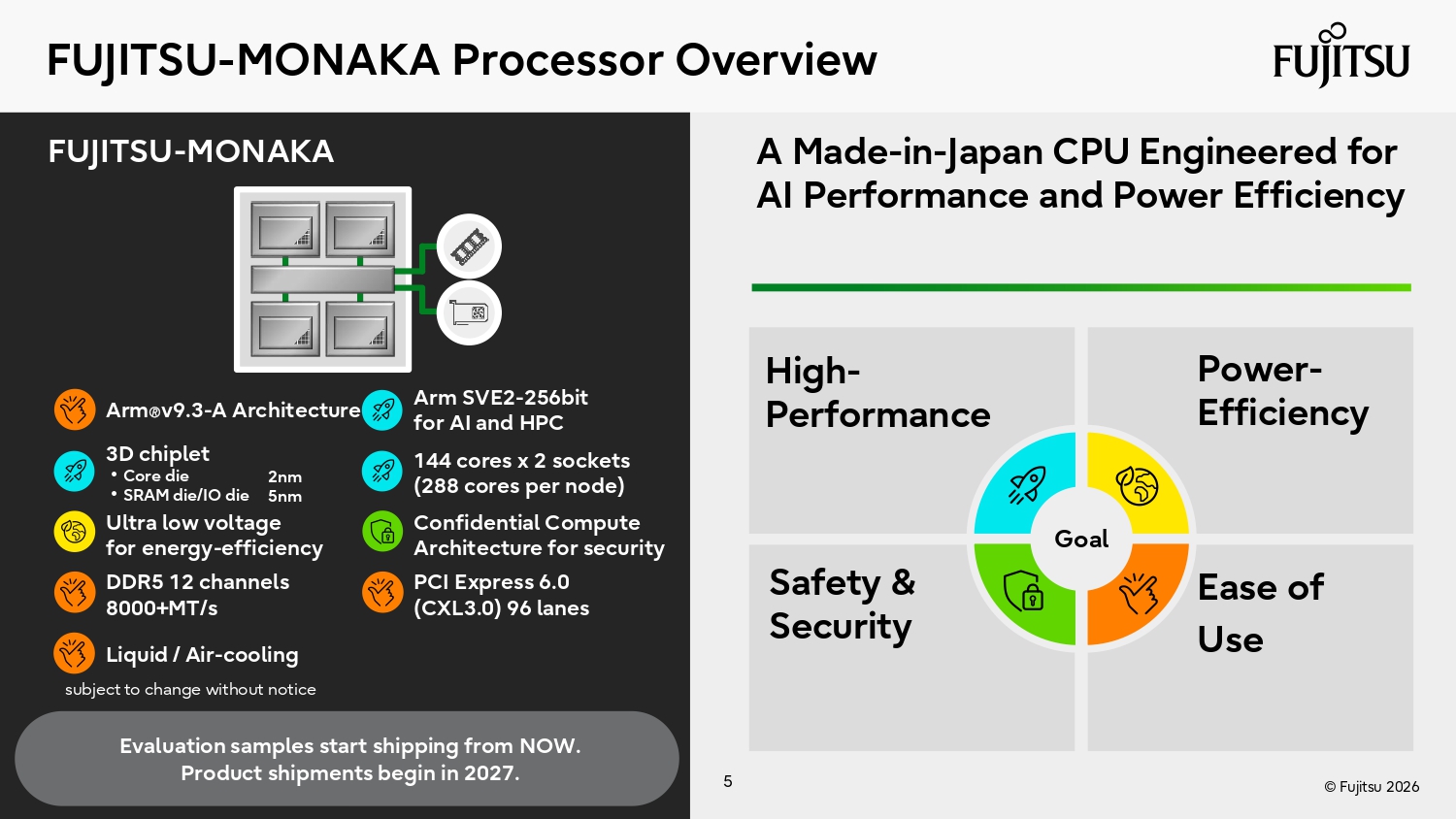
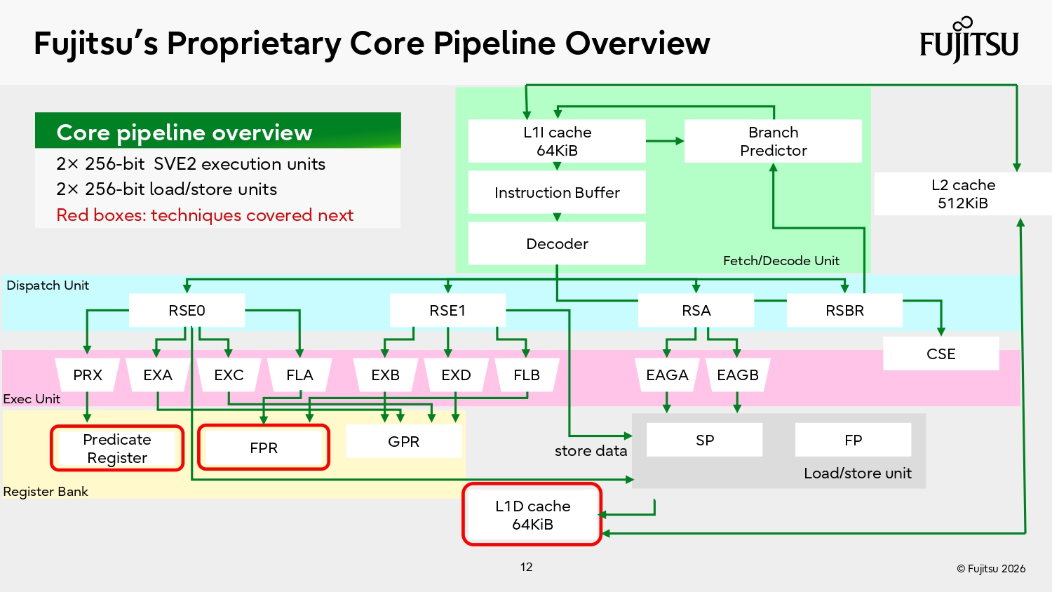
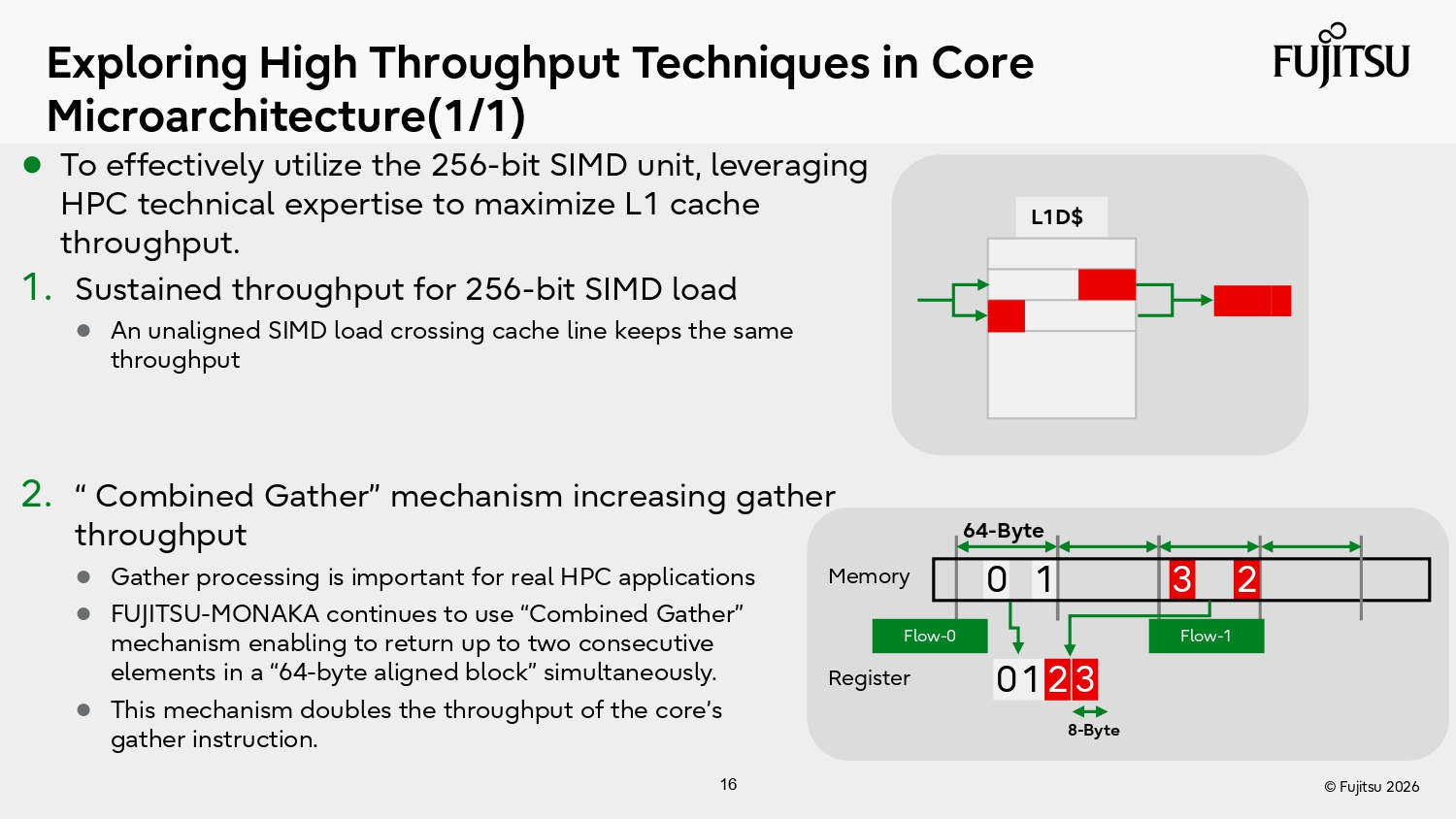
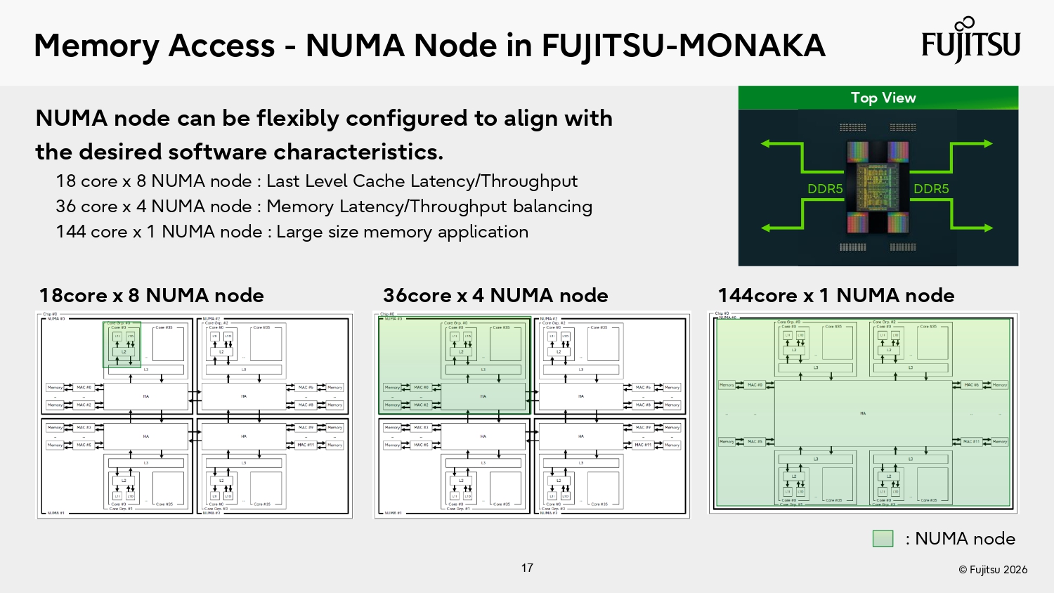
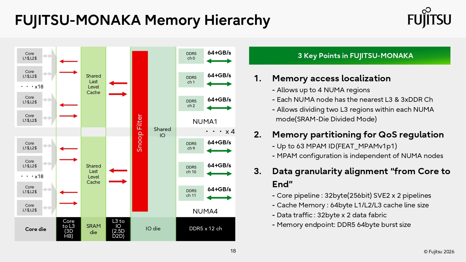
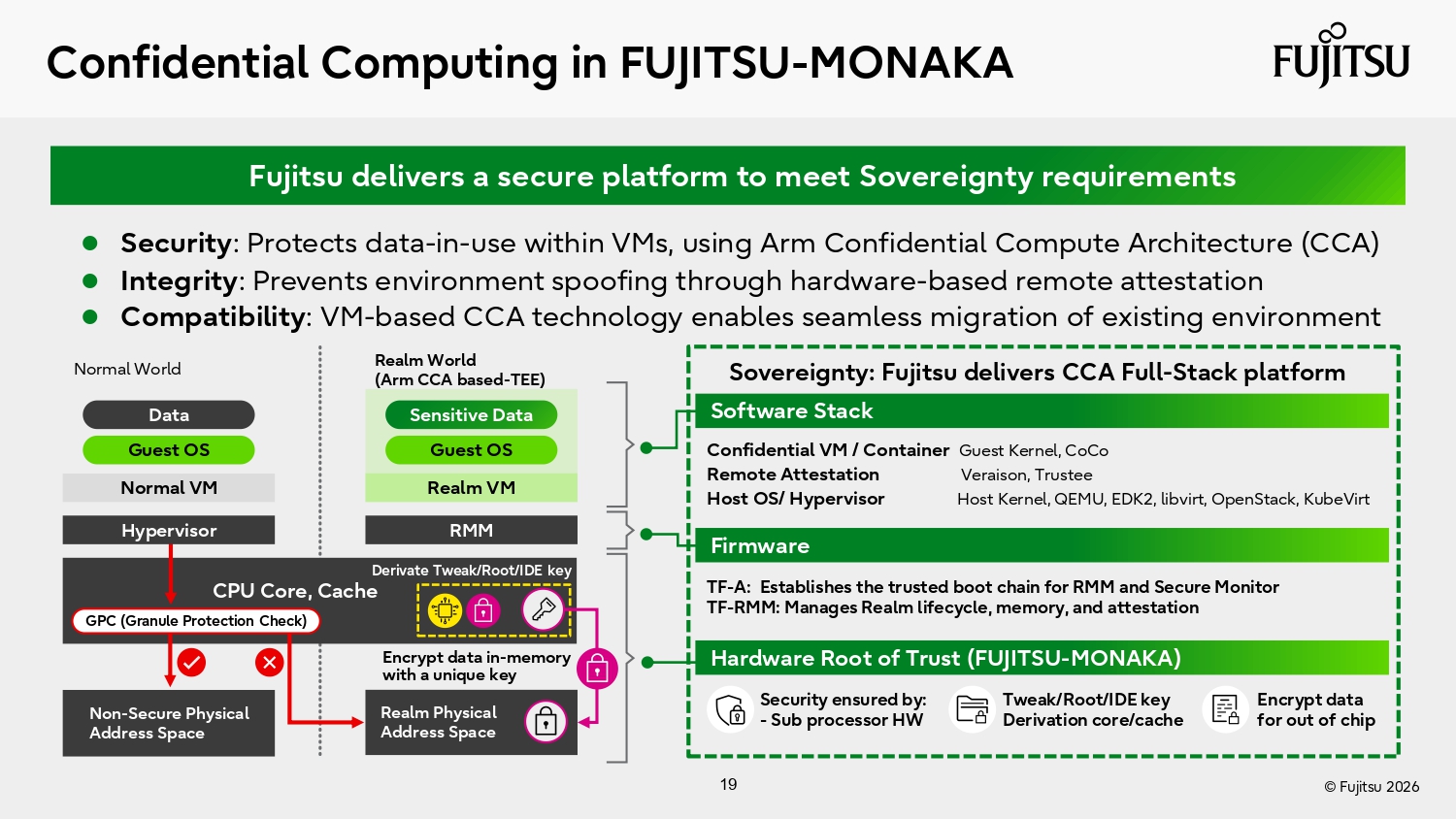
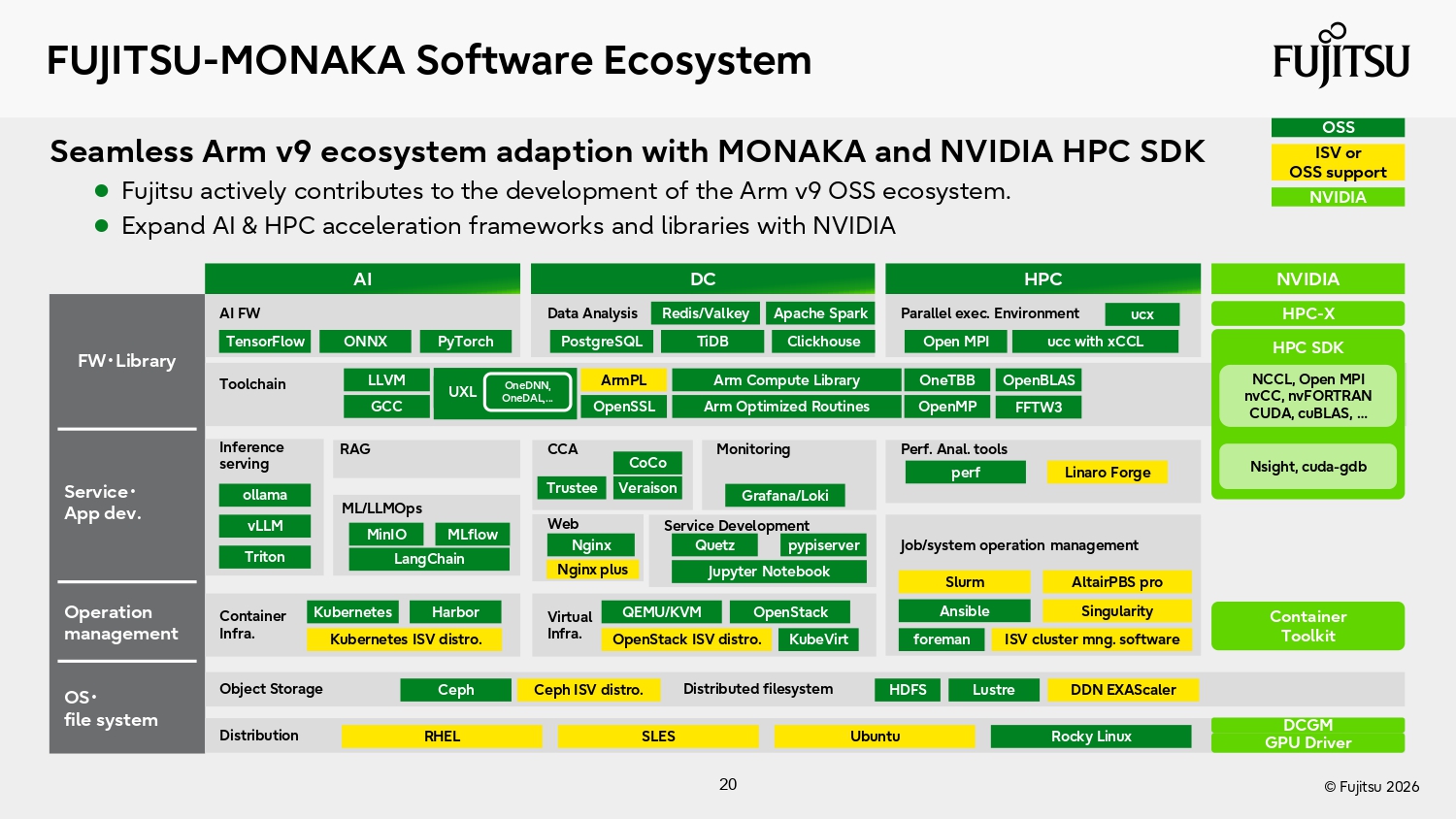
Fujitsu gave us a detailed look at its 144-core Monaka server CPU at Hot Chips 2026 on August 24, confirming for the first time that the Arm chip runs dual 256-bit SVE2 vector units, down from the 512-bit SVE in its A64FX predecessor, and that its entire last-level cache sits on a separate 5nm die beneath the 2nm compute die.
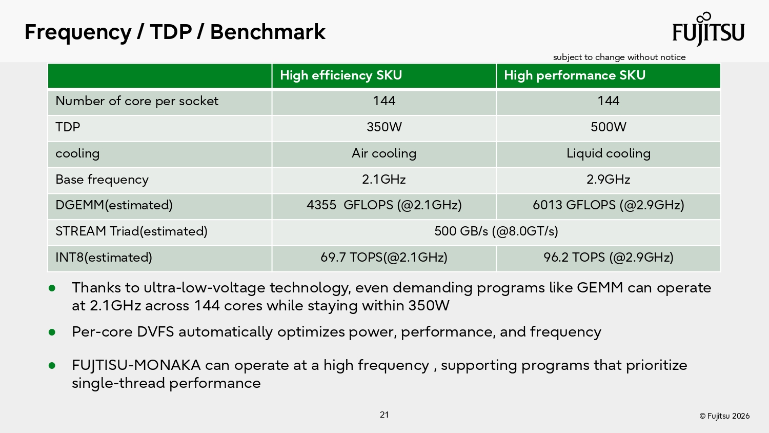
Ryohei Okazaki, lead architect of Fujitsu's processor development team, presented the design as "a made-in-Japan CPU, specifically engineered for AI performance and power efficiency," built for what the company calls green AI data centers and subsidized by Japan's New Energy and Industrial Technology Development Organization. The chip ships in two SKUs: a 350W air-cooled part at 2.1 GHz base and a 500W liquid-cooled part at 2.9 GHz base, with evaluation samples available now and volume production in 2027.
(Image credit: Fujitsu)
Three dies, one stack
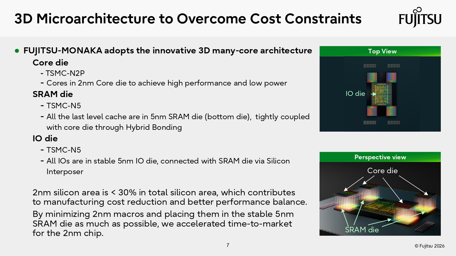
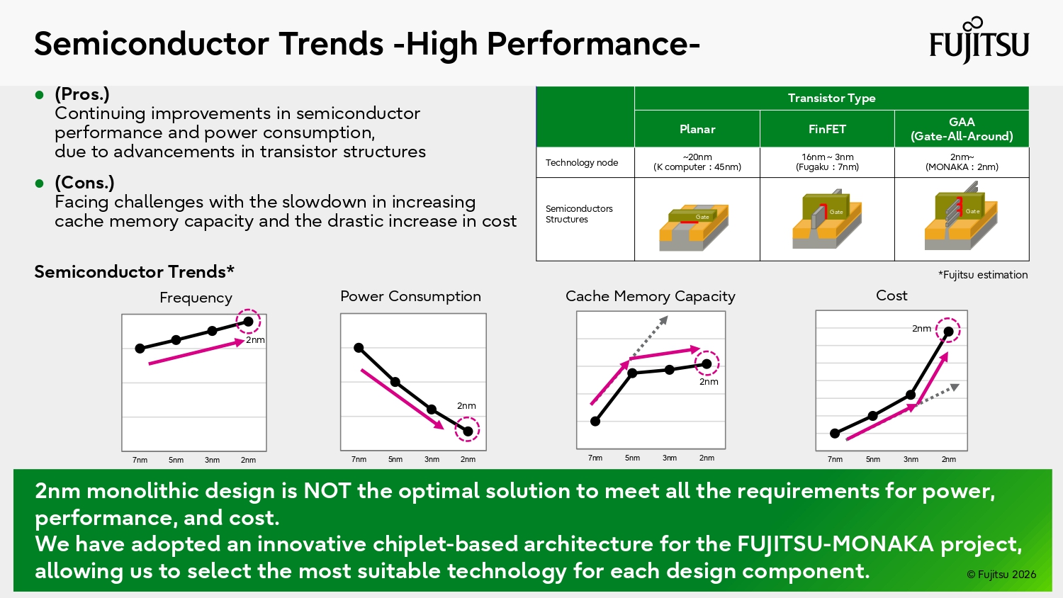
Monaka splits into three tiers of silicon: a 2nm core die on TSMC N2P, a 5nm SRAM die on TSMC N5 that holds the whole last-level cache, and a 5nm IO die. The core die stacks face-to-face on top of the SRAM die through hybrid bonding, sitting on the cooling side because it runs hottest, while the IO die connects to the SRAM die across a silicon interposer. Fujitsu keeps 2nm silicon under 30% of total die area, a split Okazaki said lets Fujitsu "accelerate the time to market for our 2-nanometer-based chip" by pushing everything that shrinks poorly onto the 5nm SRAM and IO dies.
(Image credit: Fujitsu)
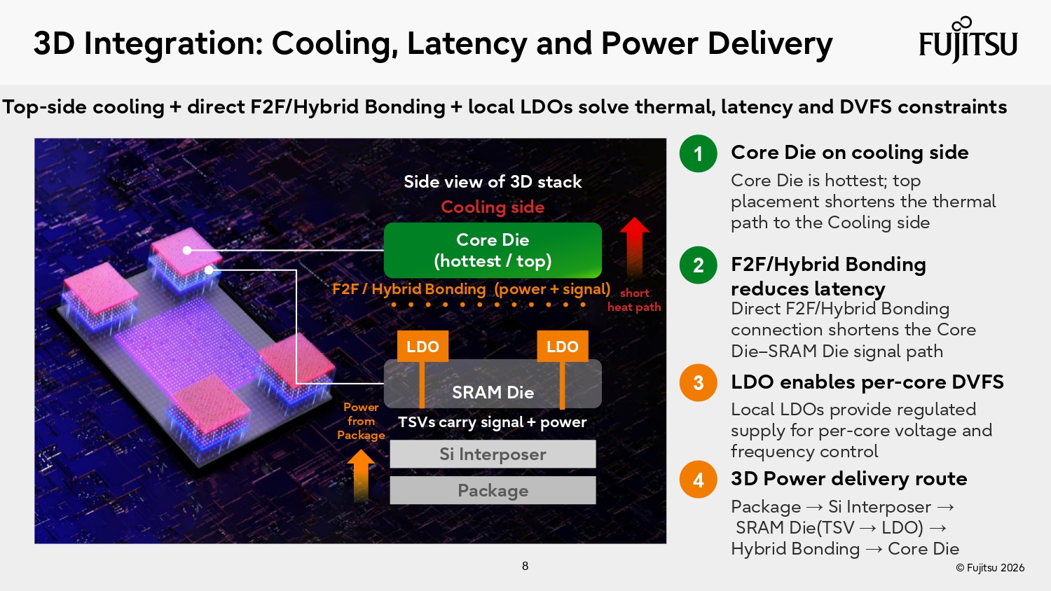
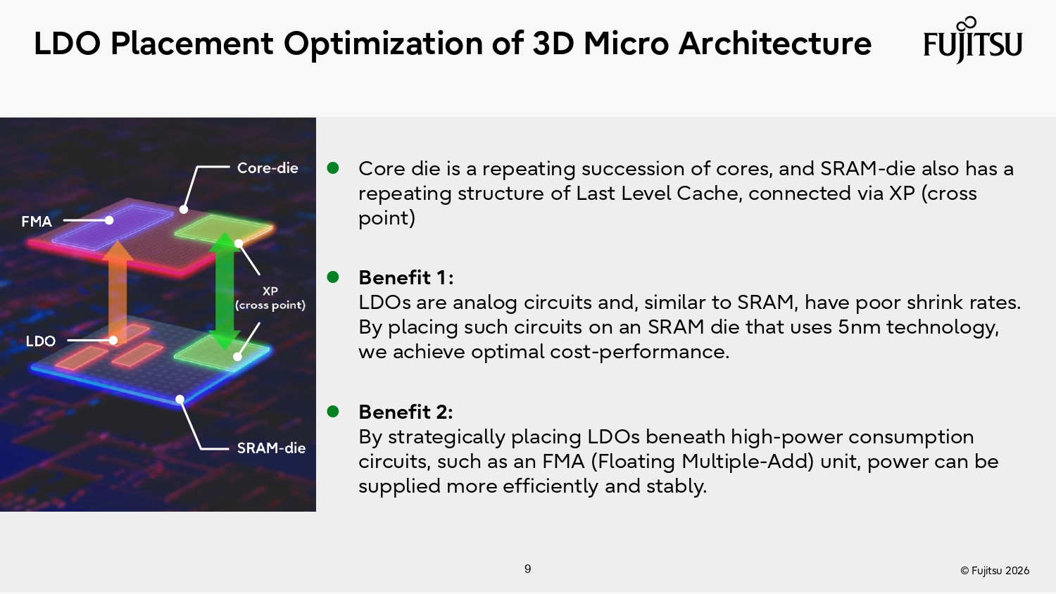
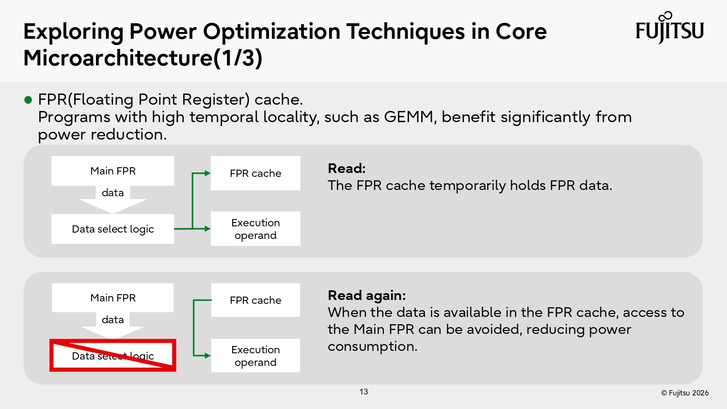
Putting the full last-level cache on a distinct stacked die separates Monaka from AMD's 3D V-Cache, which bonds extra SRAM on top of a compute die that already carries its own L3, and lines it up closer to Intel's Clearwater Forest, where local cache sits in a base tile with compute stacked above. Fujitsu also moved the low-dropout voltage regulators onto the 5nm SRAM die because analog circuits scale poorly at 2nm, and placed them directly beneath the core's floating-point units to feed per-core dynamic voltage and frequency scaling.
Dr. Ian Cutress of More Than Moore asked whether Fujitsu was "doing anything special to minimize core-to-core latency" given that the core dies sit on opposite sides of the package and traffic routes through the IO die and back. Fujitsu pointed to the face-to-face hybrid bonding between the core and SRAM dies but declined to disclose latency figures.
(Image credit: Fujitsu)
From 512-bit vectors to 256
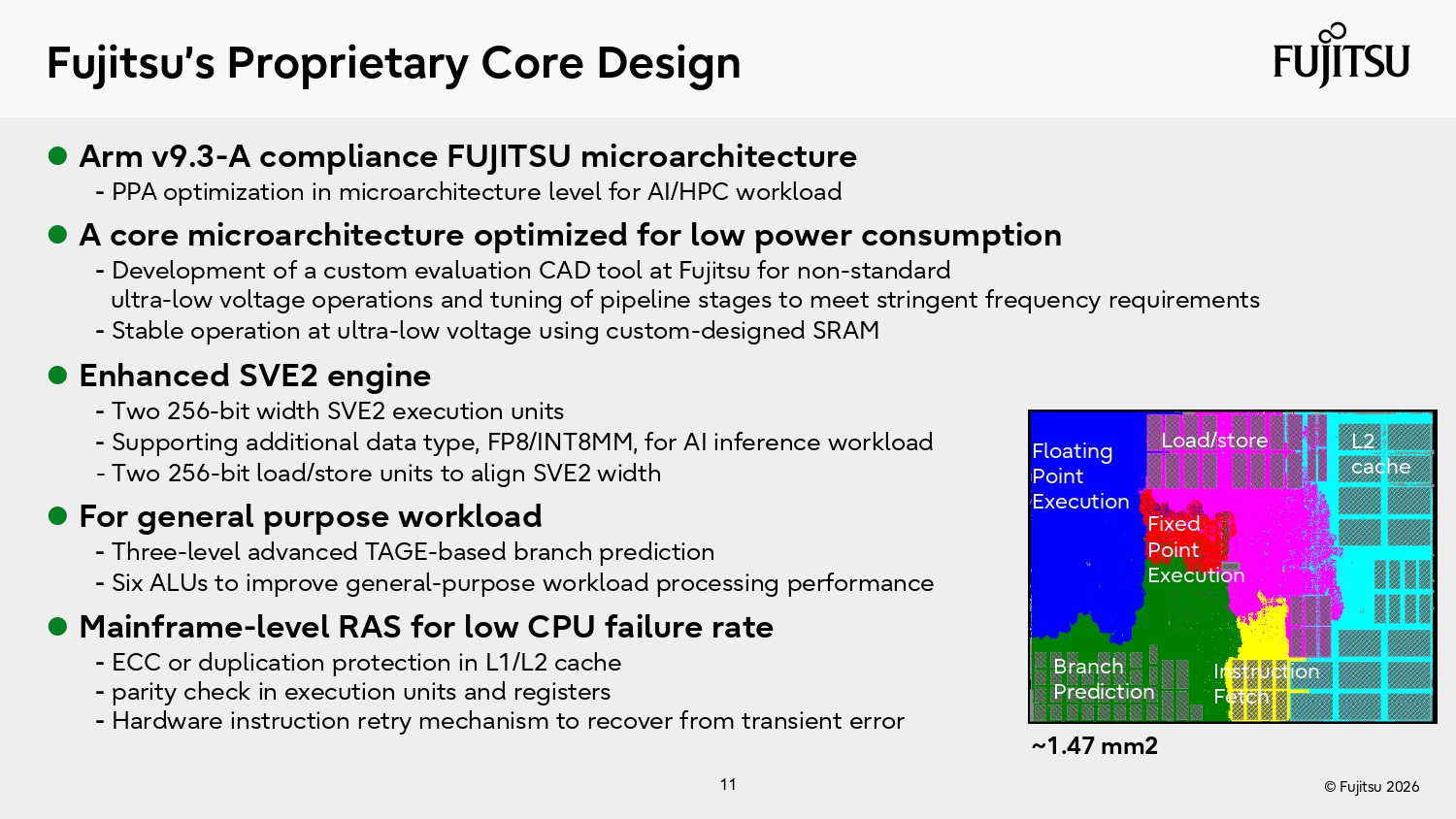
Chester Lam of Chips and Cheese asked why Fujitsu narrowed the vector datapath from the 512-bit SVE in A64FX to 256-bit SVE2 in Monaka. Okazaki said the chip is built "for [the] data center" and that Fujitsu wanted to "minimize the core size" for the best cost and performance, with the narrower units also cutting SIMD width for general-purpose code.
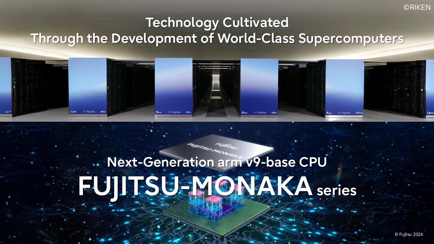
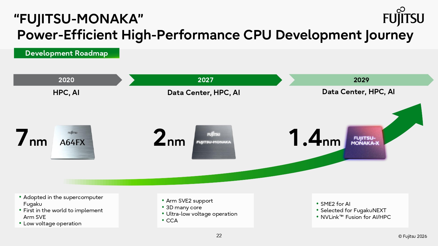
A64FX, the 7nm CPU that powered the Fugaku supercomputer and became the first chip to implement Arm SVE, paired its 512-bit vectors with on-package HBM2 for memory-bound HPC. Monaka drops HBM for 12-channel DDR5 at 8000 MT/s and runs two 256-bit SVE2 units per core, each aligned to a 256-bit load/store unit, with FP8 and INT8 matrix support added for inference.
The core carries mainframe-class reliability features Fujitsu inherited from its own processor line: ECC or duplication on the L1 and L2 caches, parity checks on execution units and registers, and a hardware instruction-retry mechanism to recover from transient errors. It also runs a three-level TAGE branch predictor and six ALUs for general-purpose throughput, on a core that Fujitsu measures at roughly 1.47 mm2.
Performance estimates and rivals
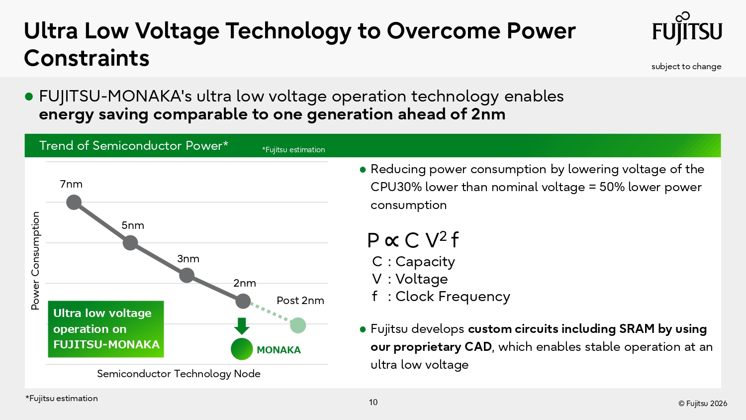
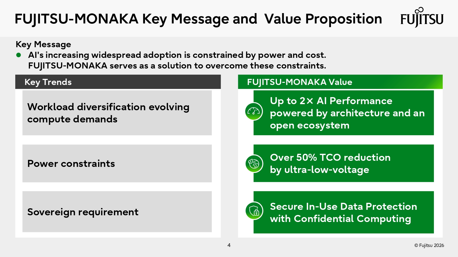
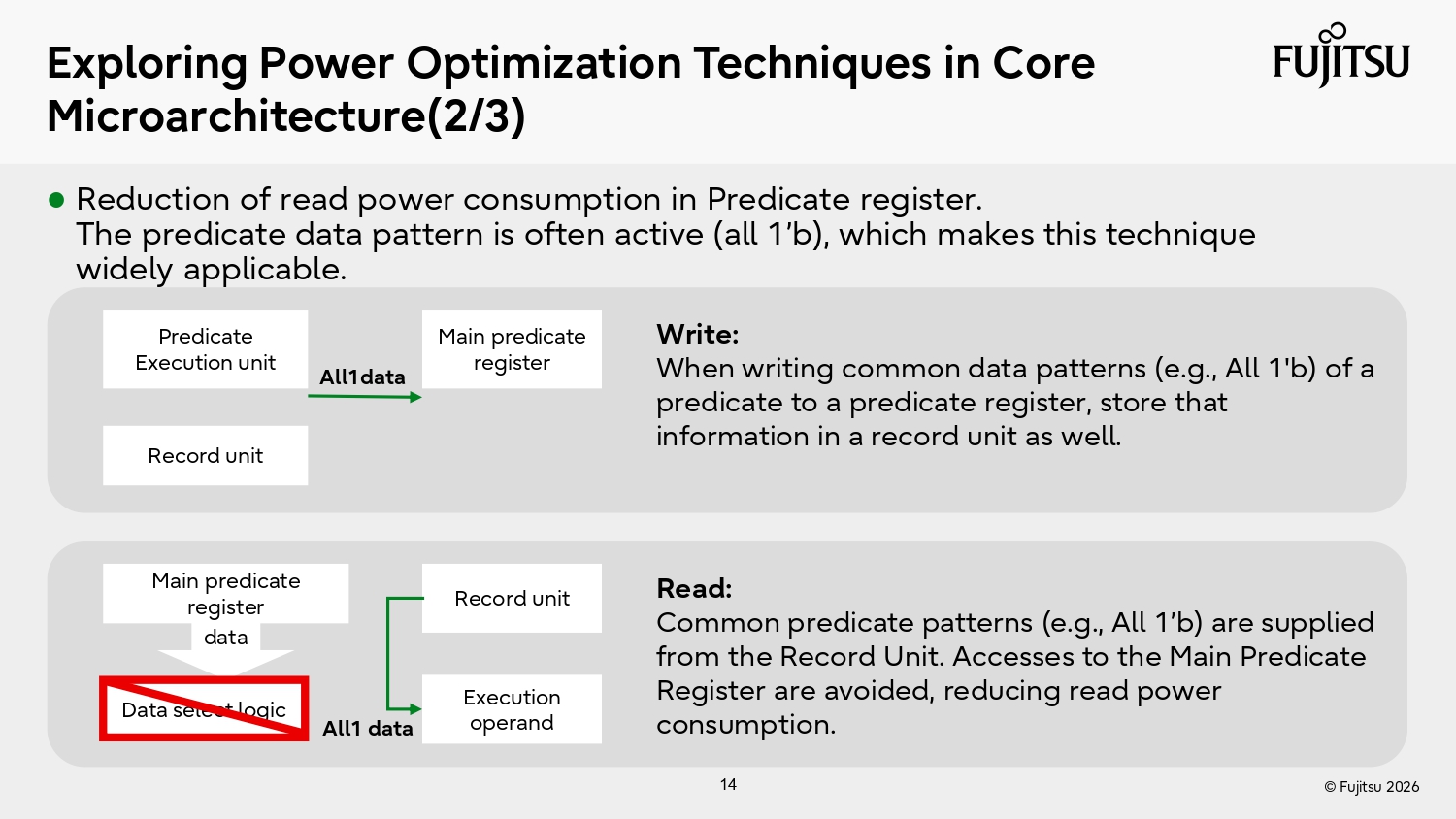
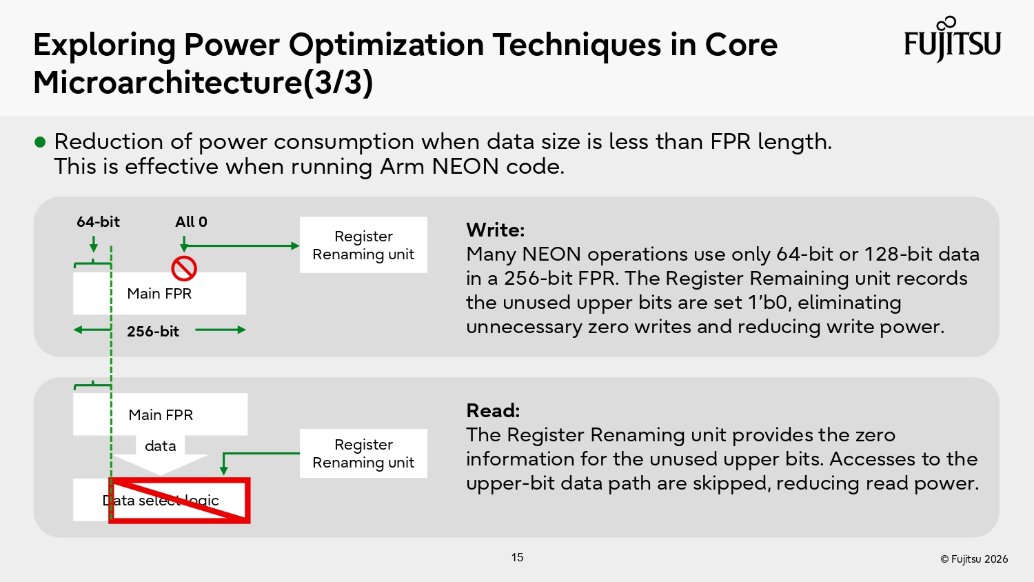
Fujitsu estimates the 350W SKU at 4,355 GFLOPS in DGEMM and 69.7 TOPS in INT8, and the 500W SKU at 6,013 GFLOPS and 96.2 TOPS, with both parts rated around 500 GB/s in STREAM Triad. The company claims up to two-times AI performance and over 50% TCO reduction against unnamed comparisons, and credits ultra-low-voltage operation, running the core around 30% below nominal voltage for roughly half the power, for holding 144 cores inside the 350W envelope. Okazaki described the voltage technique as delivering "energy saving comparable to moving one generation beyond the 2 nanometers," achieved with custom SRAM and a proprietary CAD flow tuned for non-standard low-voltage operation.
(Image credit: Fujitsu)
By 2027, Monaka's 144 cores will land in the middle of the Arm server field rather than at the top of it. AWS's Graviton5 reaches 192 Neoverse V3 cores on a single 3nm die, Ampere's roadmap runs to 512 cores in AmpereOne Aurora, and Microsoft's Cobalt 200 packs 132 cores with its own per-core DVFS. Monaka's separation from that group rests on the cache-on-die stack and 12-channel DDR5 bandwidth rather than core count, and its 256-bit SVE2 width matches SiPearl's Rhea1 while exceeding the 128-bit SVE2 common to hyperscaler Arm cores.
NEDO subsidizes Monaka under a green data center program targeting 40% energy savings by 2030, yet the chip's 2nm and 5nm dies come from TSMC rather than a domestic fab. That gap between a made-in-Japan design and Taiwanese manufacturing sits awkwardly against the sovereignty that Fujitsu and RIKEN are seemingly keen to attach to the program.
Japan has committed more than 2 trillion yen to Rapidus for 2nm production in Hokkaido by 2027, and roughly 1.2 trillion yen to TSMC's Kumamoto fabs, and NEDO has separately backed a dedicated 1.4nm AI chip from Fujitsu and IBM Japan to be built entirely in Japan by Rapidus. Monaka predates that domestic capacity, however.
Monaka's successor is already assigned to a flagship machine. FugakuNEXT, the roughly $750 million RIKEN system announced in August last year with Fujitsu and Nvidia, will pair a 1.4nm-class Monaka-X that adds Arm SME2 with Nvidia GPUs linked over NVLink Fusion, the interconnect Nvidia opened to third-party CPUs in 2025. RIKEN targets more than 600 FP8 exaFLOPS within a 40MW envelope and roughly 100 times Fugaku's application performance, with operation around 2030. FugakuNEXT is Japan's first flagship supercomputer to place GPUs at its core, a departure from the CPU-only A64FX design of the original Fugaku.
(Image credit: Fujitsu)
Fujitsu has firmed up rather than changed the Monaka plan across three years of disclosures, with the core count, node split, and an anticipated launch date of 2027 remaining unchanged since 2023. Fujitsu didn't disclose pricing, and its DGEMM, STREAM, and INT8 figures remain estimates until independent testing at the 2027 launch
When Arm introduced its AGI data center CPU, which it will ship starting in late 2026, the company revealed key specifications but omitted many technical details. It said nothing about the processor's performance at the time. This week at Hot Chips 2026, Arm filled many gaps about the architecture and design decisions of its AGI CPU, disclosed that the processor works as planned, published planned configurations, and said it is on track for commercial shipments in the coming months.
Many cores
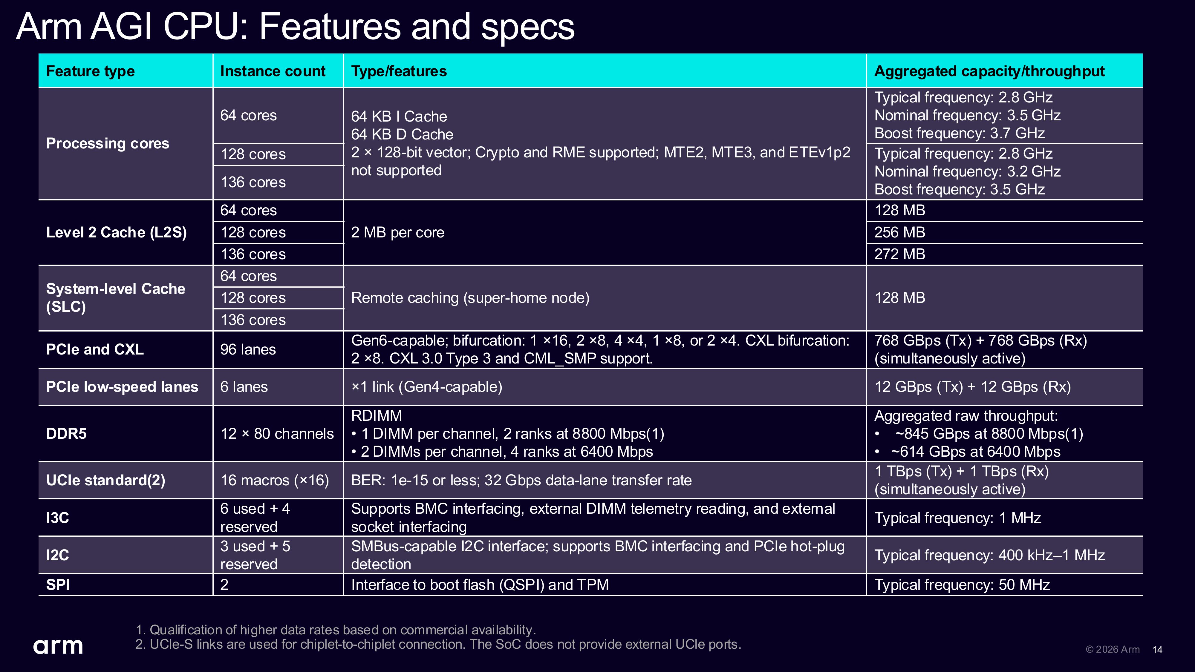
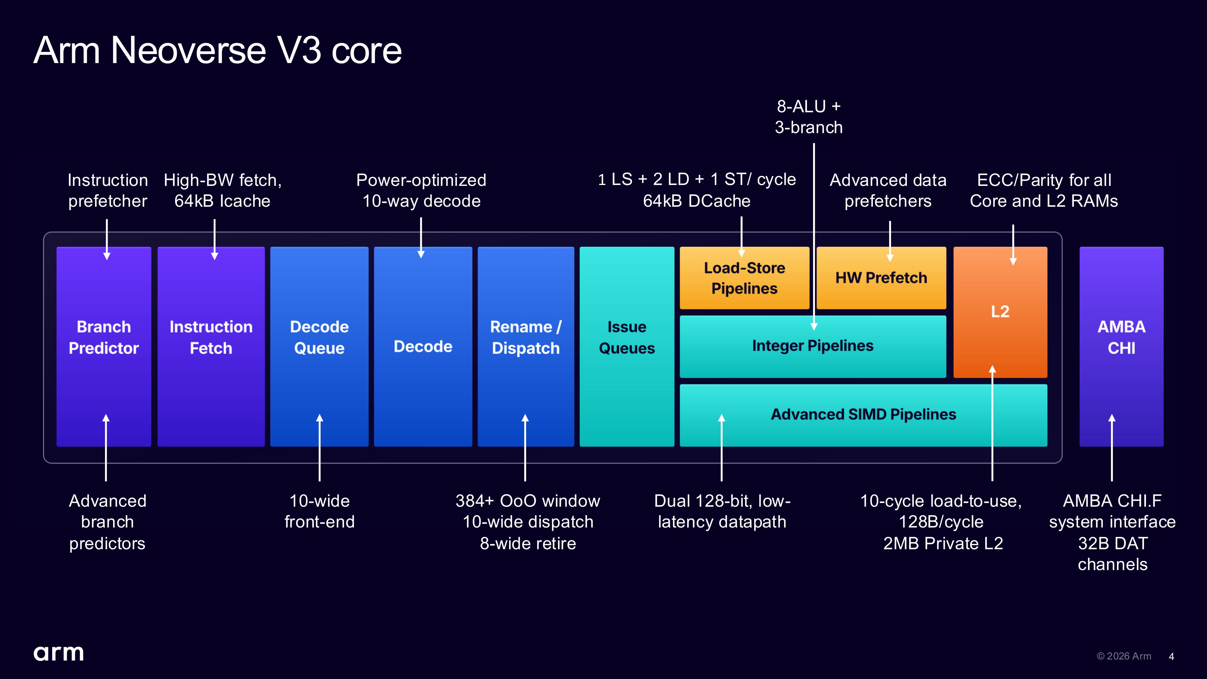
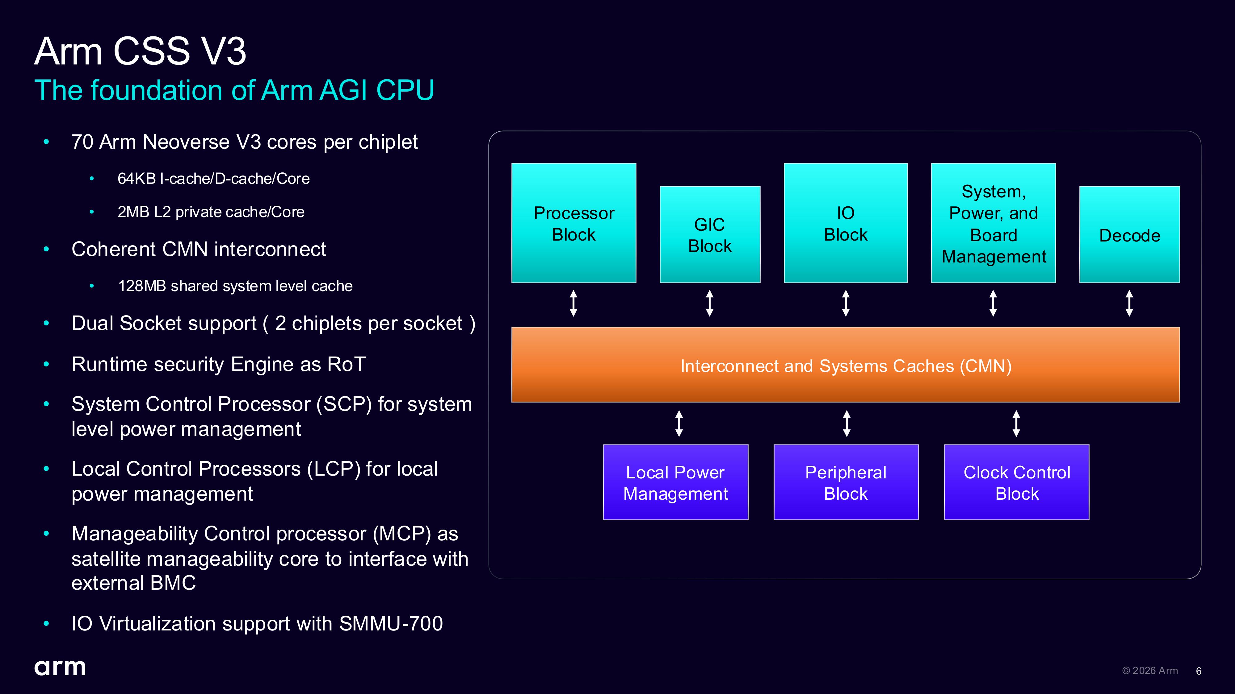
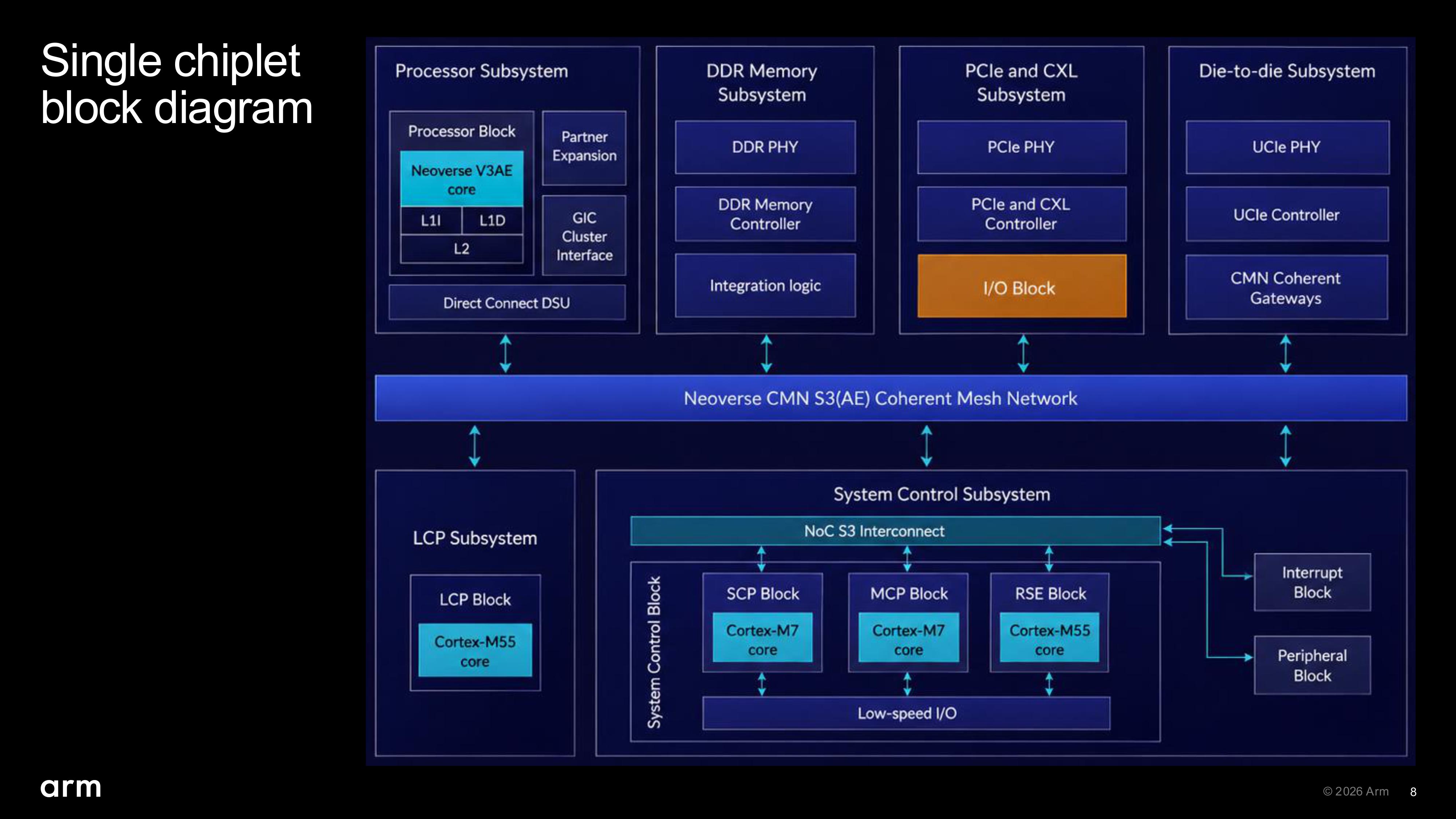
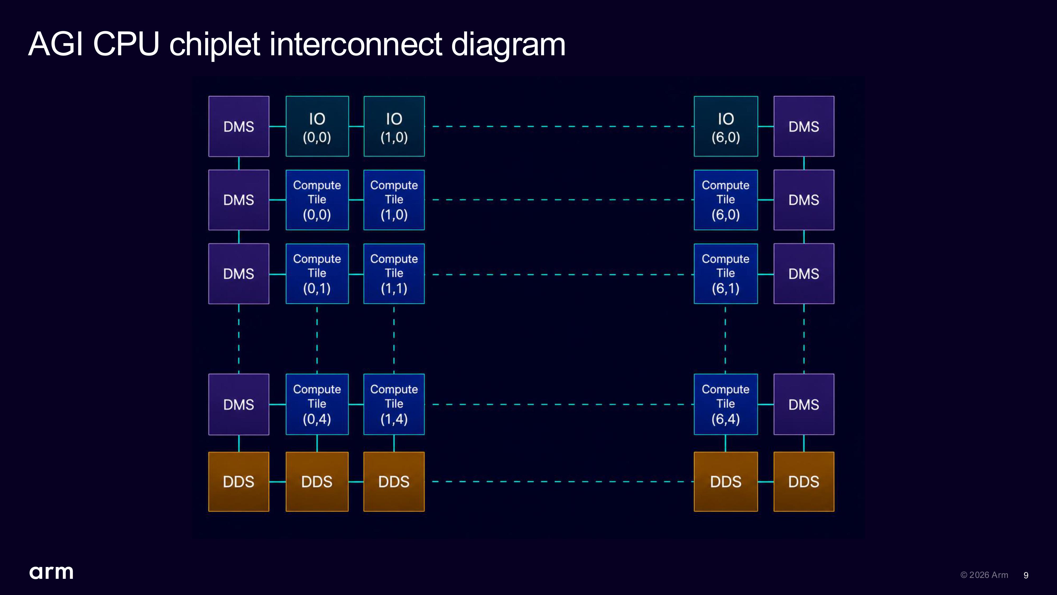
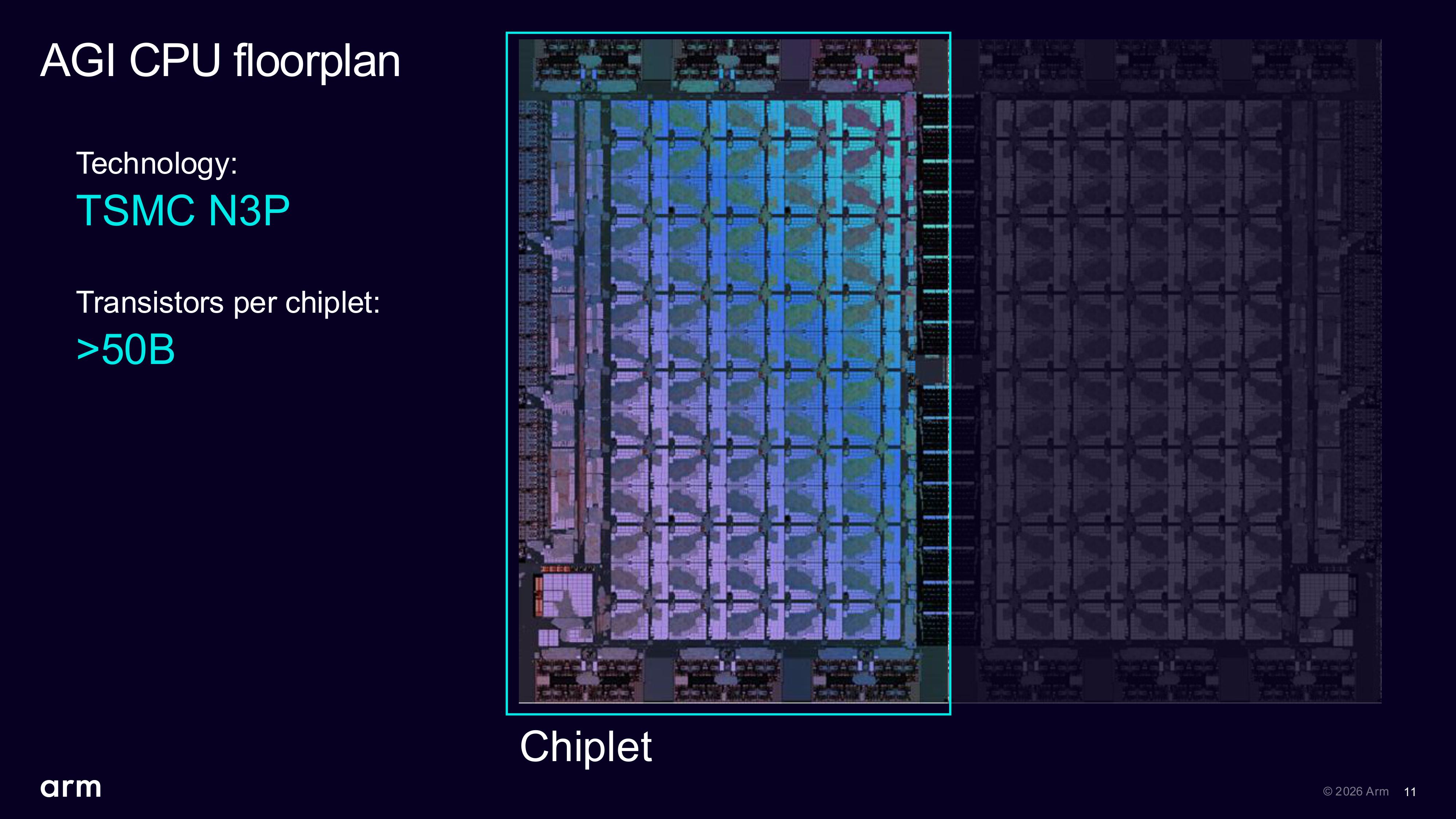
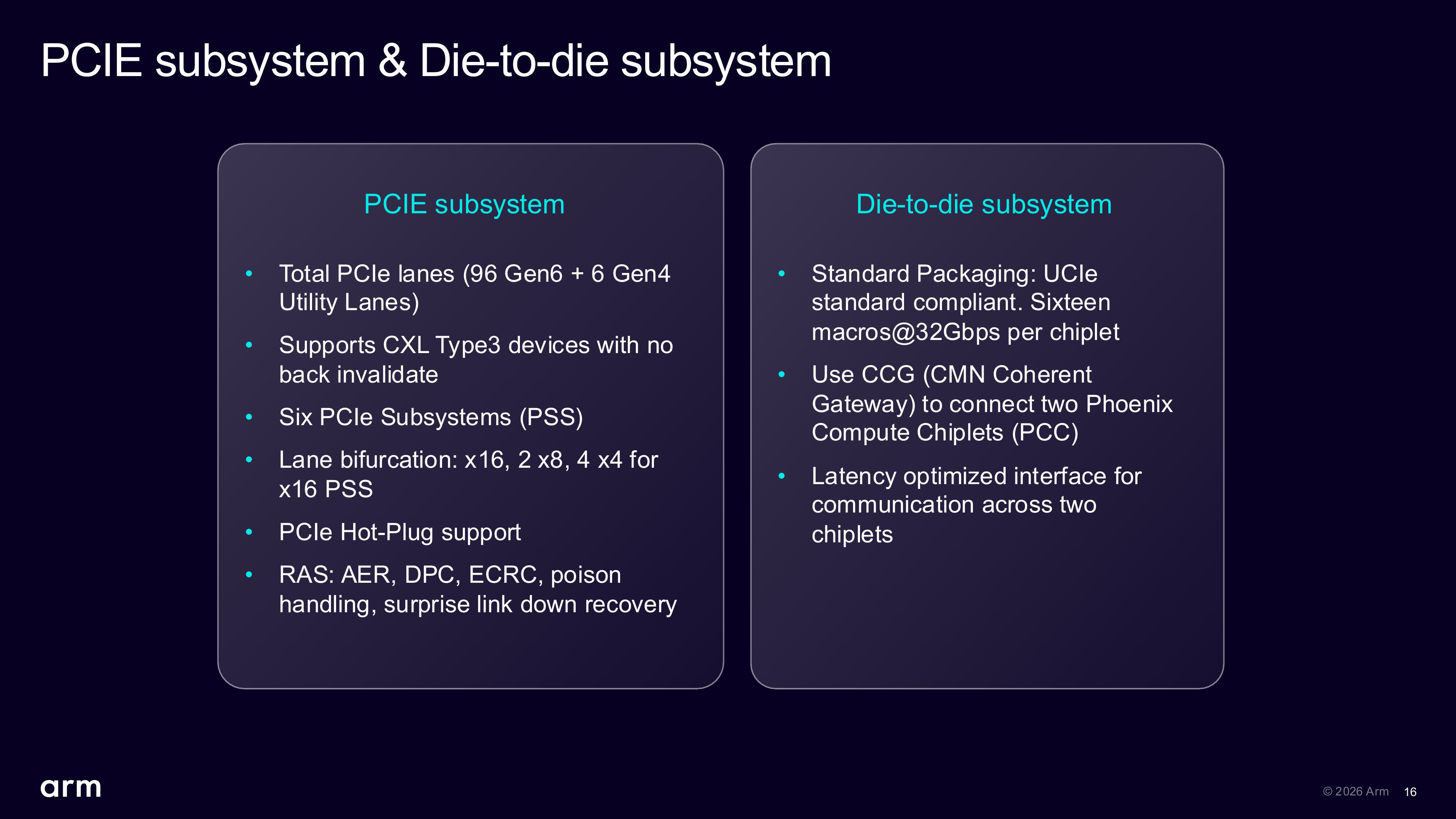
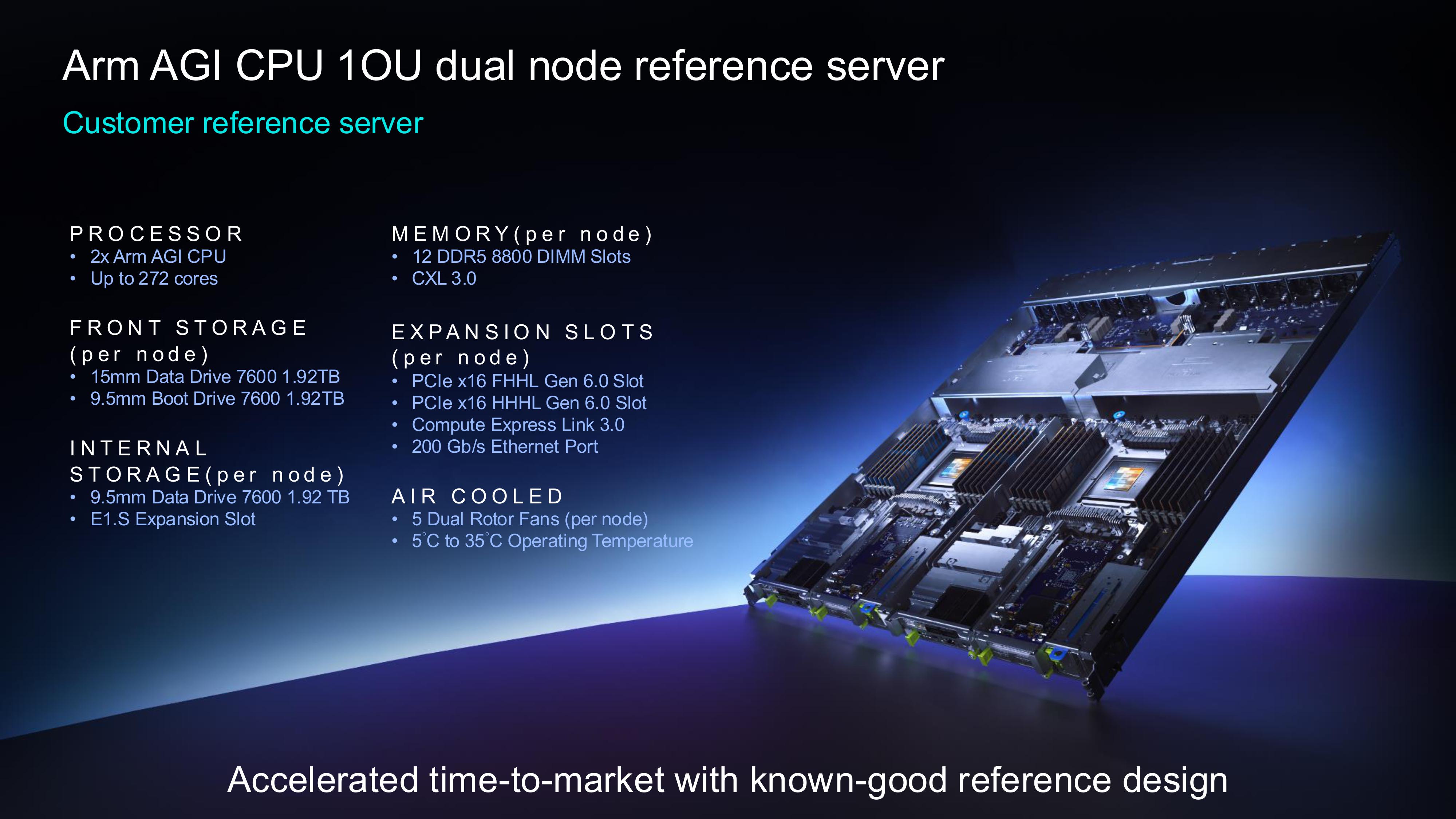
Arm's AGI is a dual-chiplet data center processor that packs 64, 128, or 136 Neoverse V3 cores (10-wide frontend and decode, 10-wide dispatch, 8-wide retire, 384+ entry OoO window) running at 2.80 GHz – 3.70 GHz. The processor is equipped with two 128-bit vector engines and 2MB of L2 cache per core, as well as up to 272 MB of system-level cache. Each CSS V3 chiplet consists of 50 billion transistors, contains 70 V3 cores, a six-channel memory subsystem supporting up to 3 TB of DDR5-8800 memory (6 TB per socket), and connects to its sibling using a 16 ×16 UCIe macros running at 32 GT/s with an aggregated bandwidth of 2 TB/s. On the I/O side of things, Arm's AGI has 96 PCIe 6.0 lanes utilizing the CXL 3.0 protocol on top for memory expansion, four PCIe 4.0 lanes, and I3C, I2C, and SPI interfaces. The CPU has a thermal design power of 300W.
(Image credit: Arm)
At a high level, Arm's AGI does not look too different from CPUs from AMD, Intel, and Nvidia: it has many cores, plenty of cache, a high-performance memory subsystem, and dozens of PCIe lanes with CXL. However, several design choices from Arm buck some usual trends from other CPU makers.
Unorthodox design choices
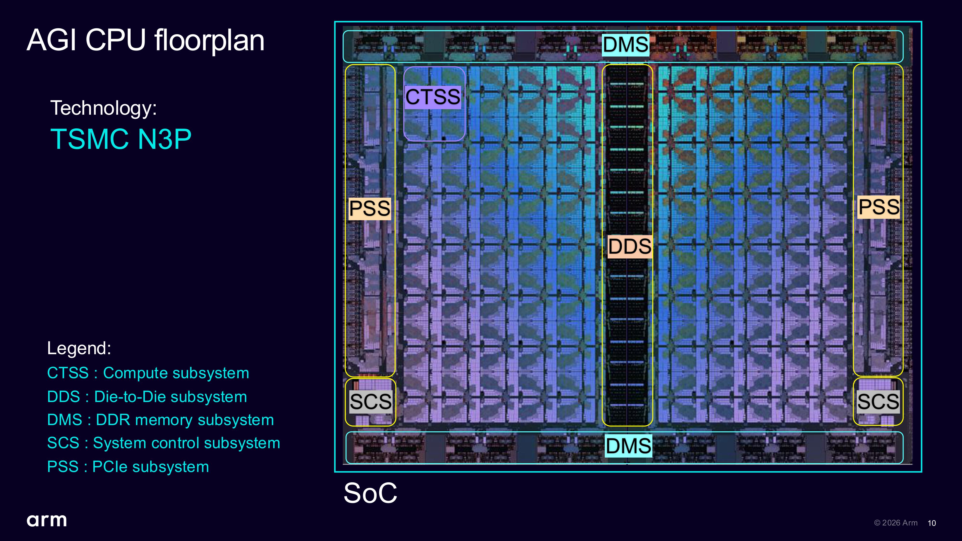
The first thing that catches the eye is that Arm chose two largely self-contained SoC chiplets made on TSMC's N3P technology, which places both compute and I/O on the same die, and decided not to go with the usual heterogeneous multi-chiplet designs used by AMD, Intel, and now Nvidia, all of whom separate compute and I/O chiplets.
While AMD, Intel, and Nvidia use their heterogeneous multi-chiplet approach to pack more compute capability and deliver more performance, it looks like Arm's decision is fundamental to its combination of enormous memory bandwidth (844.8 GB/s when used with DDR5-8800, though such memory still has to make it to the market) and
(Image credit: Arm)
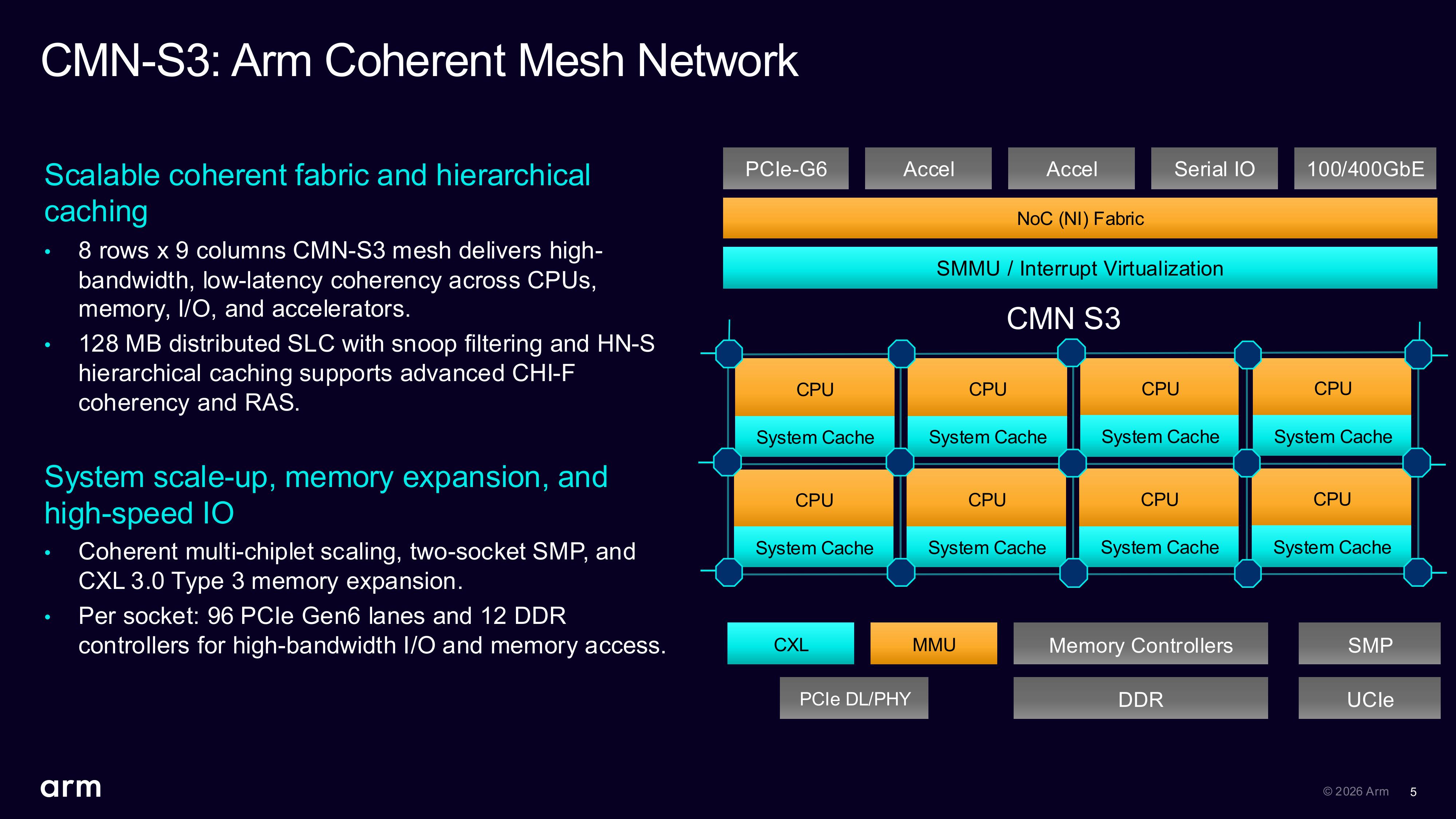
Each chiplet uses an 8 × 9 CMN-S3 mesh (a low-latency interconnect) to connect CPU cores, memory, I/O, and accelerators. It incorporates a 128 MB distributed system-level cache, snoop filtering, and hierarchical caching through HN-S, or Super Home Node, a piece of logic that acts as a distribution center for handling traffic and data through the chip to speed up communication.
The important point is that CMN-S3 is not just an internal CPU mesh, as Arm designed the coherent system to extend outside of the die to extend coherency beyond the die and the socket. The approach is conceptually closer to Intel's distributed Xeon 2D mesh (though Xeon is moving on to a 3D mesh with Diamond Rapids) than AMD's EPYC architecture, where compute chiplets connect to a central I/O die that hosts the memory controllers and Infinity Fabric infrastructure. This essentially proves that Arm appears to have optimized AGI's chiplets for memory locality, bandwidth, and latency, but not exactly for compute performance density, modularity, yield, and ease of manufacturing like AMD.
Arm revealed at Hot Chips that each chiplet physically contains 70 Neoverse V3 cores, but the complete product exposes up to 136 cores, which means that four cores are redundant and are incorporated to increase yield.
Capable memory subsystem
Arm positions its AGI CPU primarily for AI servers and agentic AI systems, in particular. Since memory performance plays a big role in many agentic AI workloads, Arm implemented a capable coherent NUMA memory subsystem. The NUMA subsystem features two six-channel DDR5 subsystems located in each chiplet, which can potentially provide a total of up to 845 GB/s of bandwidth. If a core needs memory attached to the other chiplet, the request can cross the coherent die-to-die connection, though at a cost of latency. Arm's goal is to provide as much bandwidth per core as possible, which is why AGI supports everything up to DDR5-8800.
(Image credit: Arm)
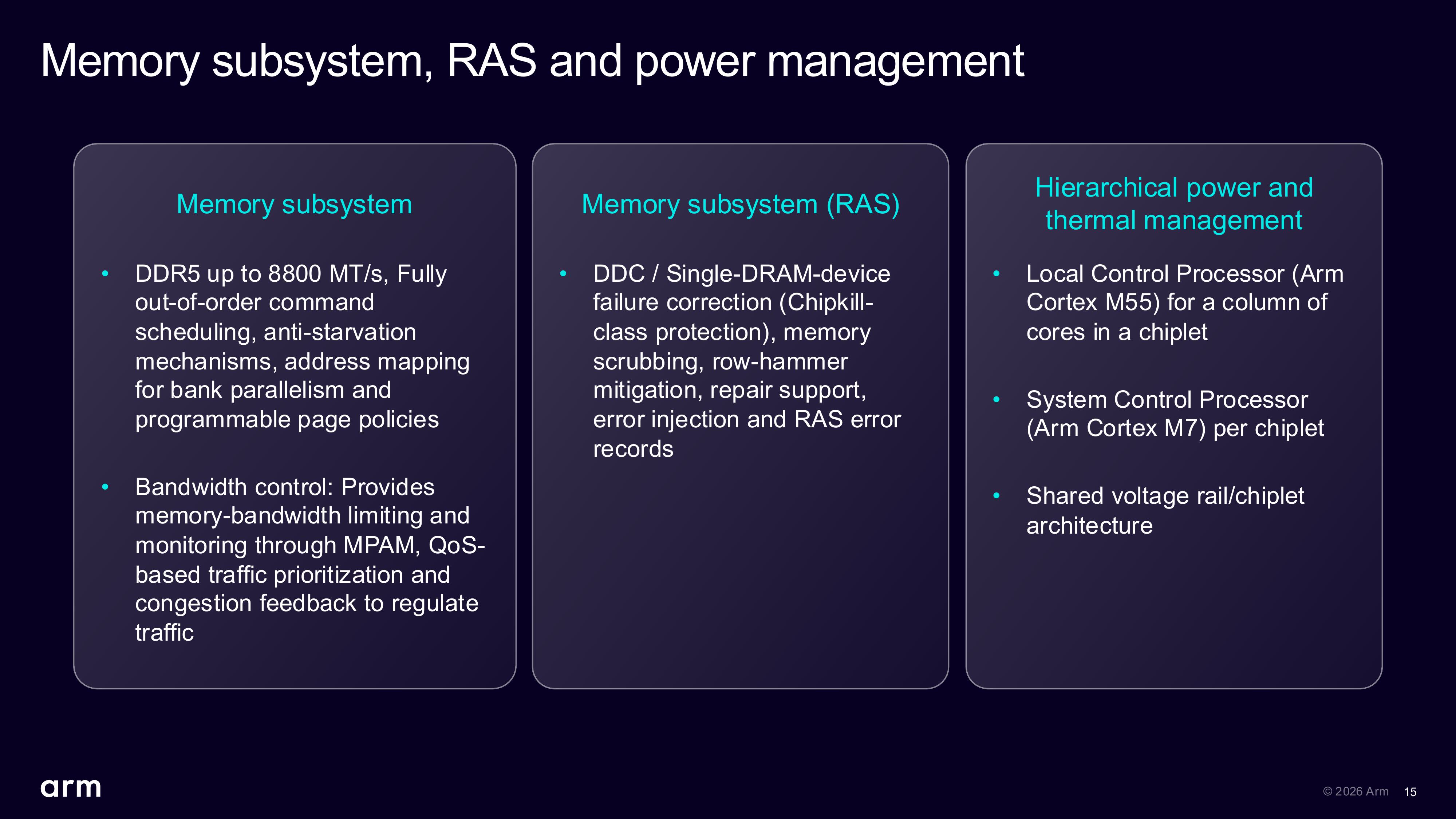
The DDR5 controllers within Arm's AGI CPU are quite sophisticated too. They support numerous features to maximize performance in real-world workloads, including fully out-of-order command scheduling, bank-parallelism-optimized address mapping, and programmable page policies to improve DRAM utilization and extract more effective bandwidth from the memory subsystem, while anti-starvation mechanisms help maintain predictable service under heavy load.
In addition, Arm also implements memory-bandwidth limiting and monitoring through Memory Partitioning and Monitoring (MPAM) along with QoS-based traffic prioritization and congestion feedback to manage contention when multiple cores and I/O devices compete for DRAM bandwidth. The memory subsystem also features extensive RAS capabilities, including single-DRAM-device failure correction with Chipkill-class protection, memory scrubbing, row-hammer mitigation, repair support, error injection, and RAS error logging.
Capable memory subsystem
Now that Arm has shared so many details about its AGI CPU, the lingering question is the performance of the processor itself. Arm still has not published conventional benchmark results such as SPEC CPU2017, SPECrate, integer/floating-point throughput, or direct socket-to-socket comparisons against current AMD EPYC or Intel Xeon processors in real-world server workloads.
The main performance claim that Arm has made is '2X performance per rack versus the latest x86 platforms' based on estimates, which is not even remotely a detailed performance claim. Perhaps, following Nvidia's lead, Arm prefers to compare the per-rack performance of its CPUs, as they are made to work in racks. However, this is clearly an unconventional way to evaluate processors.
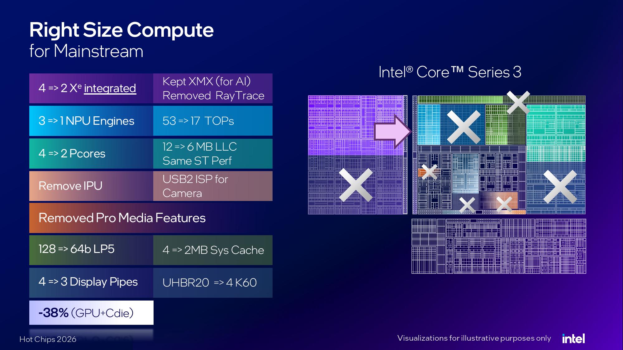
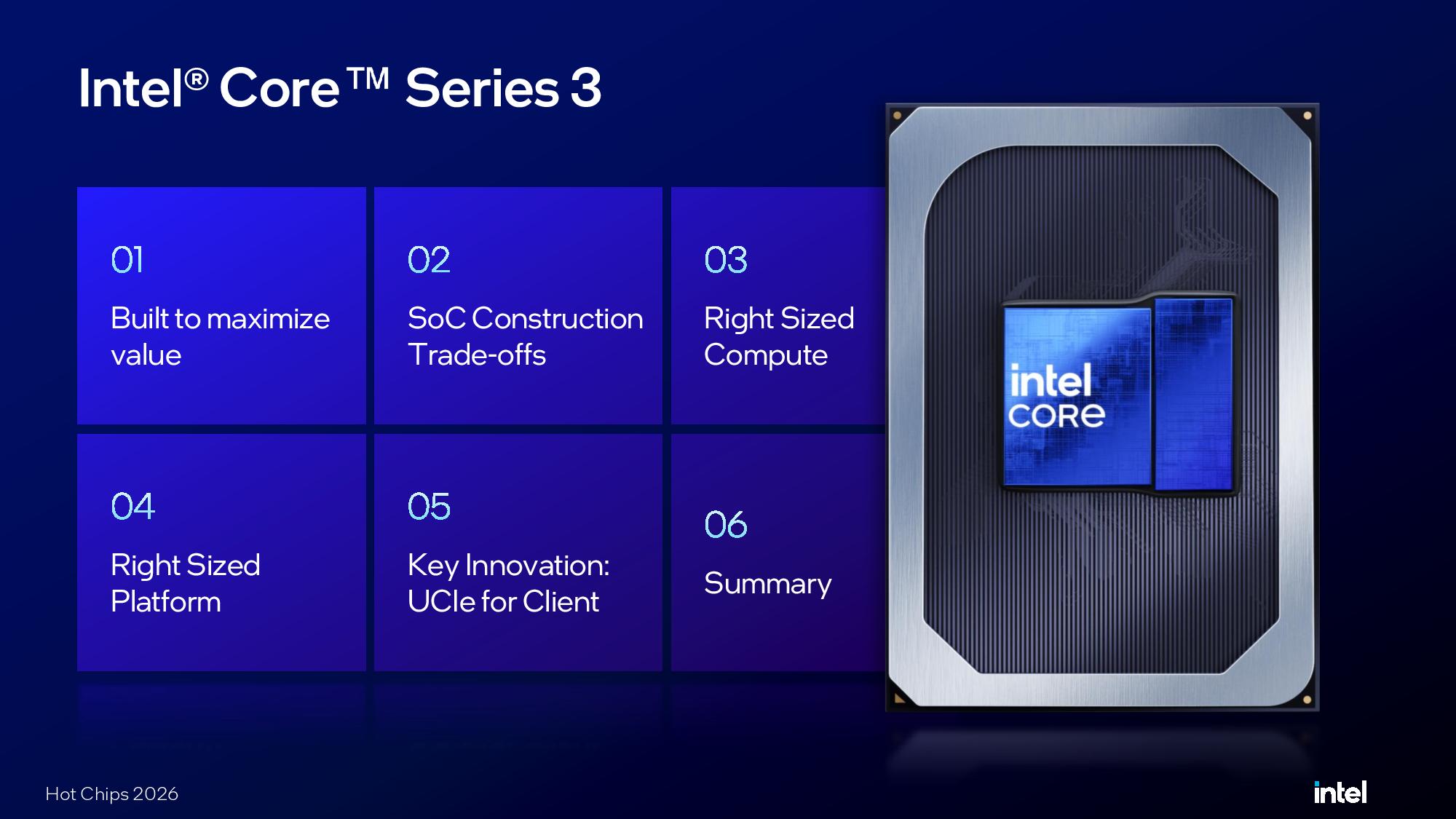
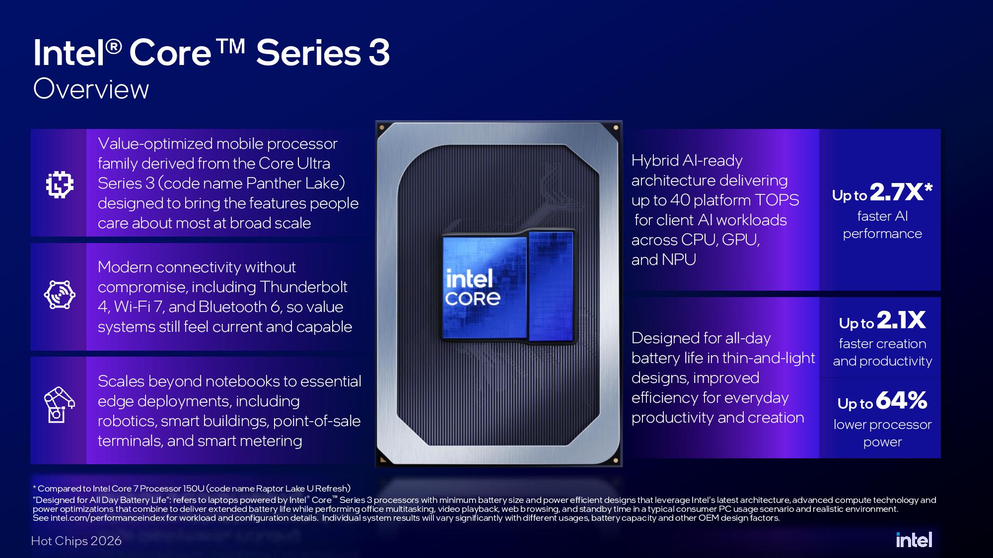
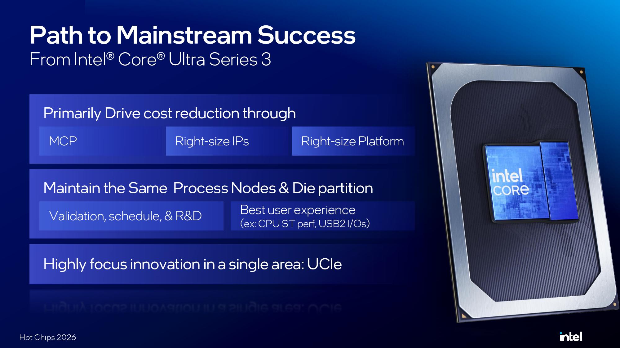
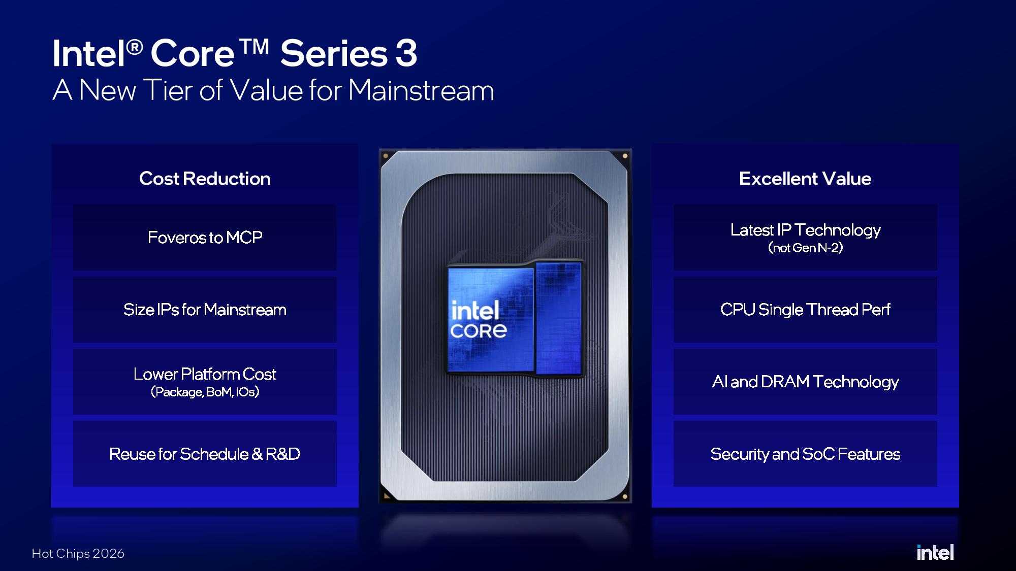
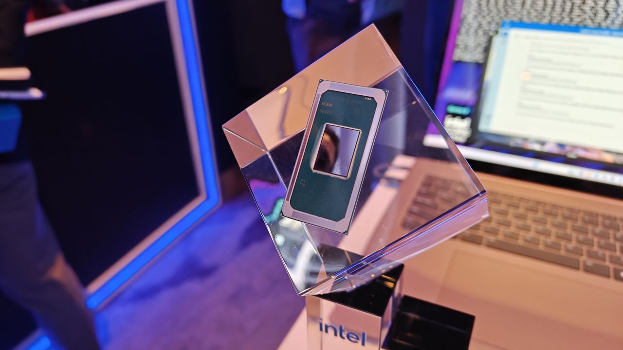
Intel's Wildcat Lake is unassuming, launching with the message that it was a cutting-edge alternative to the MacBook Neo with Intel's latest node and some trimmings around the edges. Although Wildcat Lake is, indeed, a budget part with major concessions to reach a market increasingly pushed to the side by powerful PC hardware, it also comes with a major innovation: UCIe.
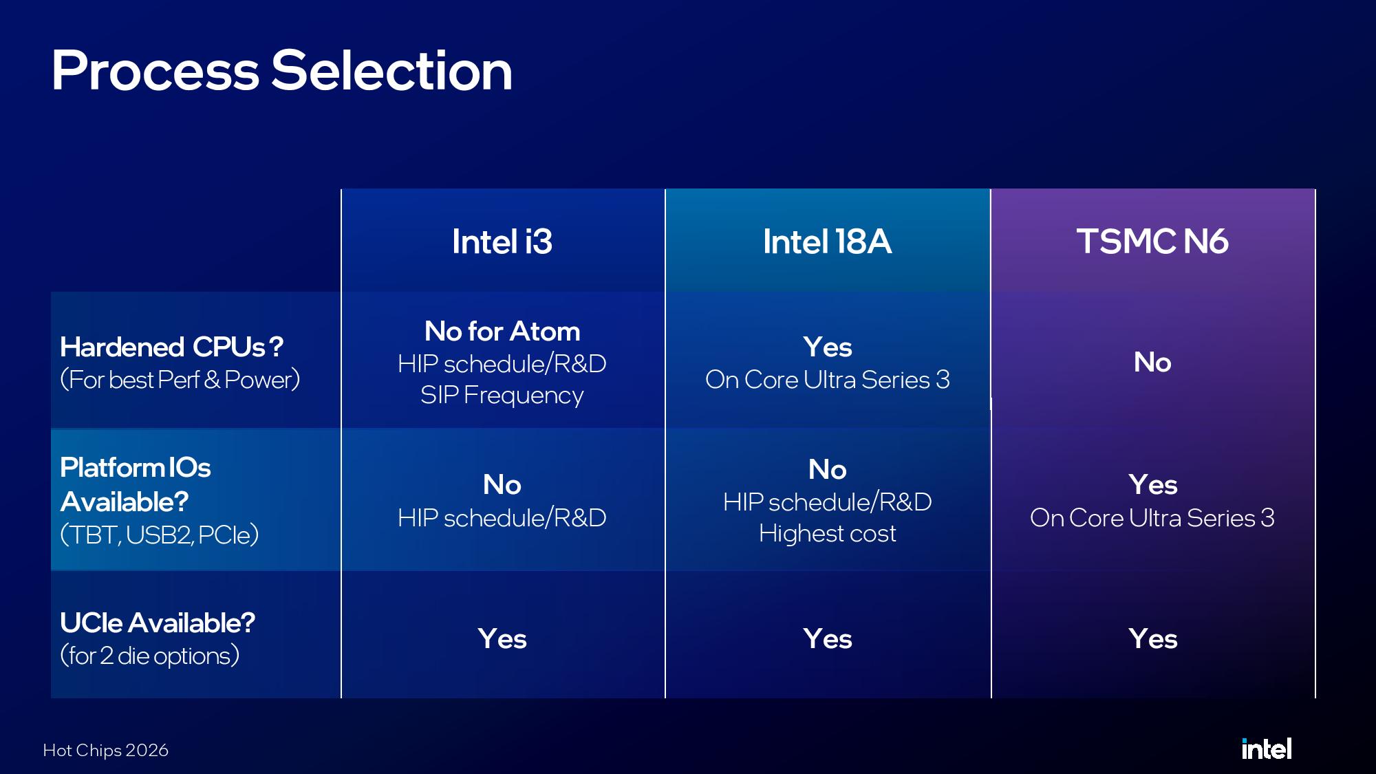
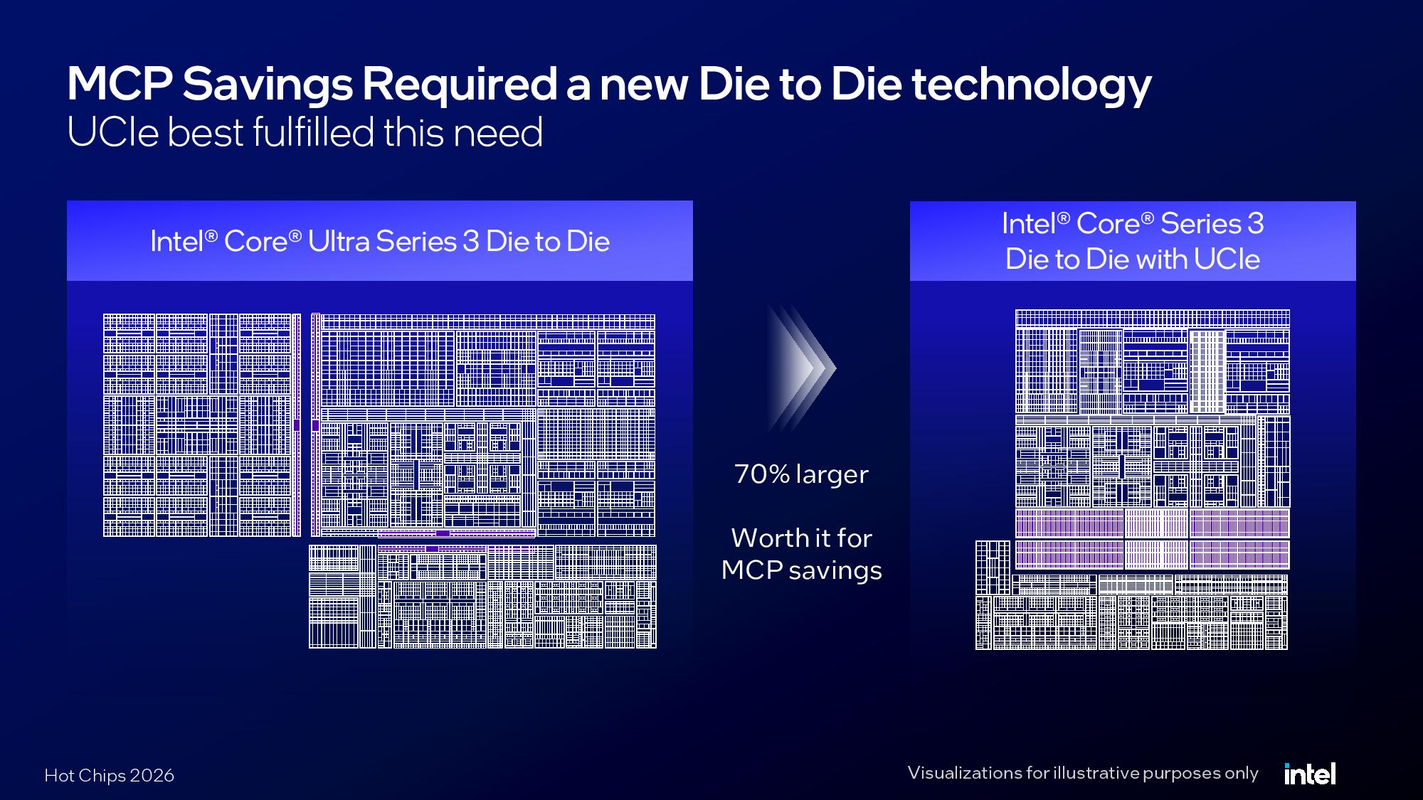
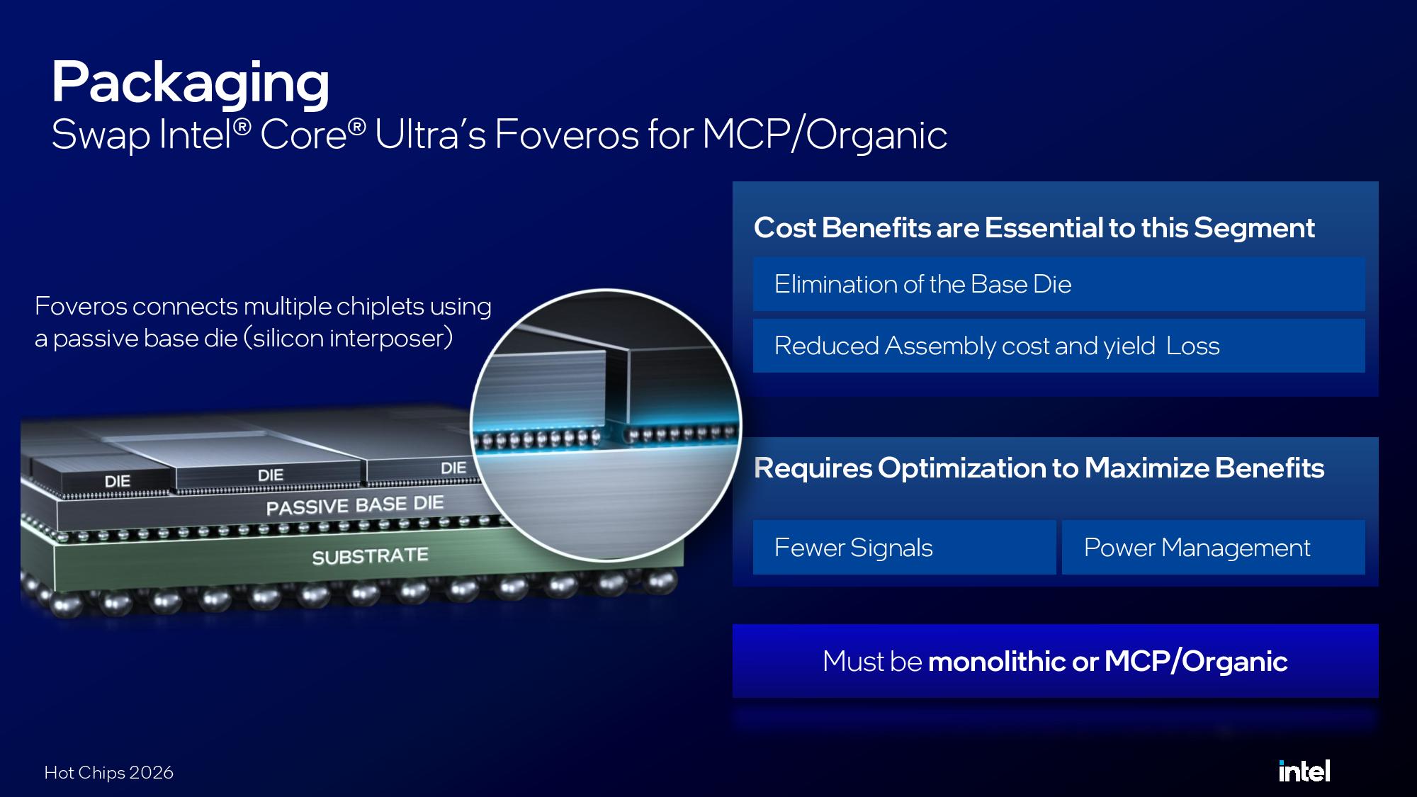
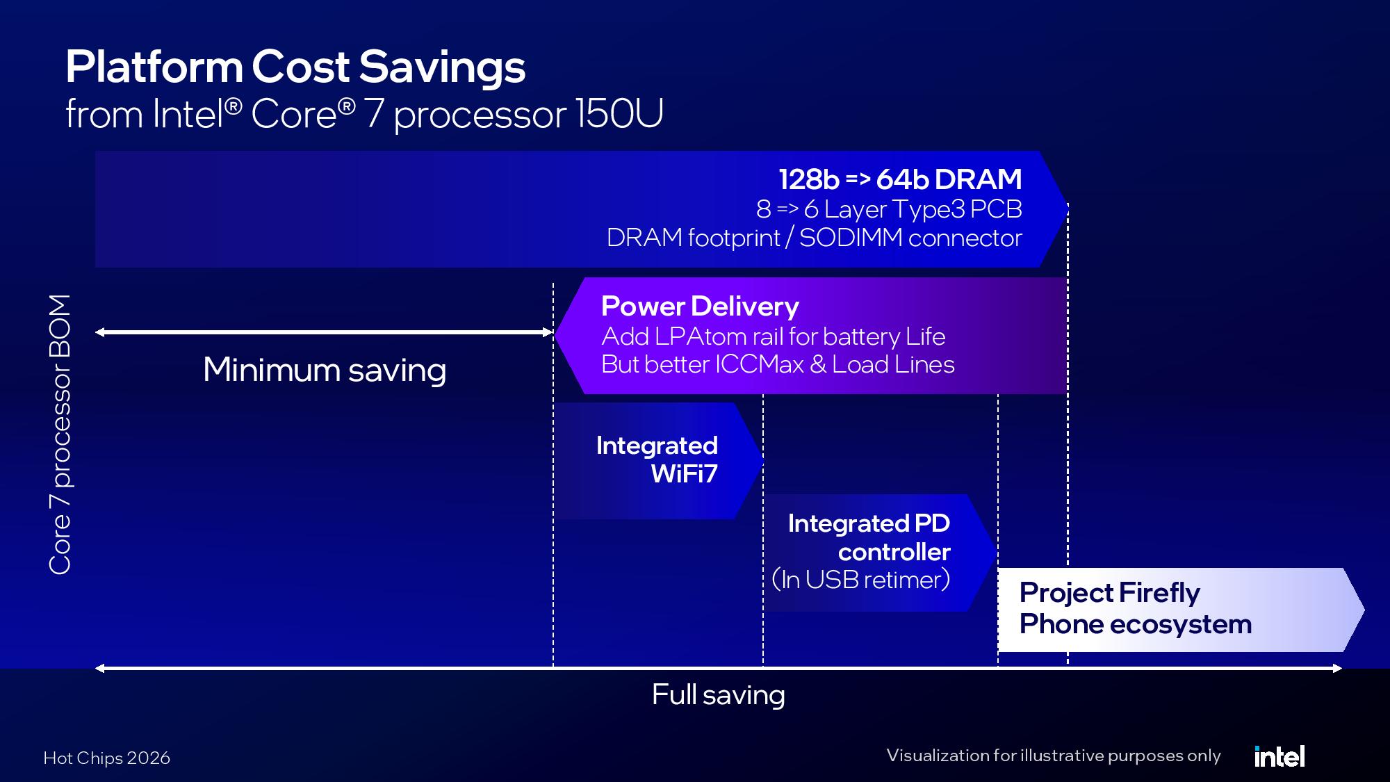
The Universal Chiplet Interconnect Express (UCIe) specification first debuted in 2022, coincidentally around the time that planning around Wildcat Lake began. Both AMD and Intel have rallied behind UCIe as an open interconnect communications standard, though they've primarily relied on their own chiplet communication technology like AMD's Infinity Fabric. In Wildcat Lake, Intel leveraged UCIe to reduce cost. Further, it was a key technology that allowed Wildcat Lake to exist in the first place.
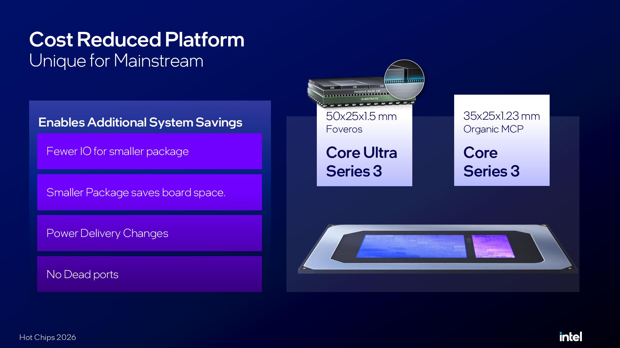
Opening the Hot Chips 2026 presentation, Intel's Lance Hacking, lead engineer on Wildcat Lake, said the company had the choice between a monolithic design or a basic, low-cost Multi-Chip Package (MCP). Intel has Foveros for advanced 2.5D and 3D packaging, but for a budget part like Wildcat Lake, that wasn't an option.
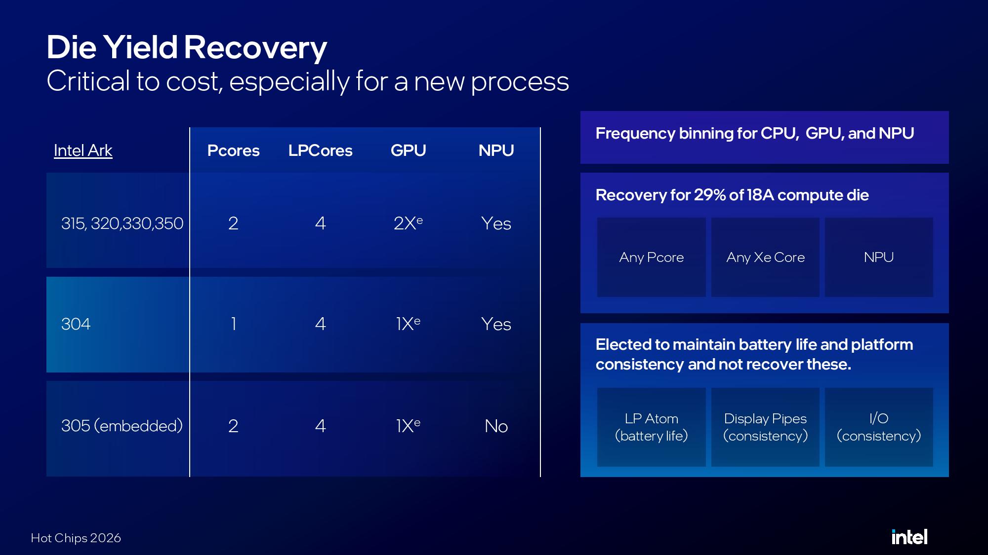
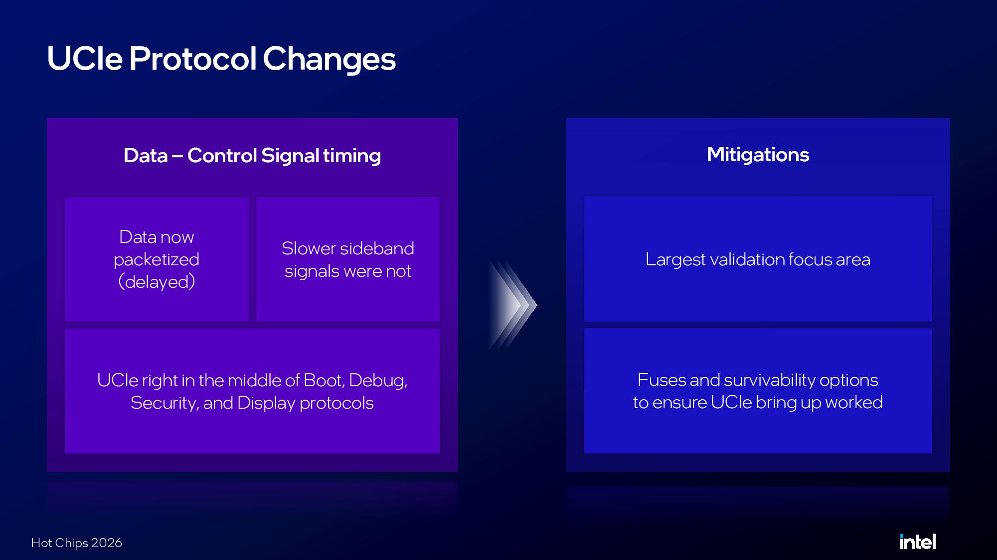
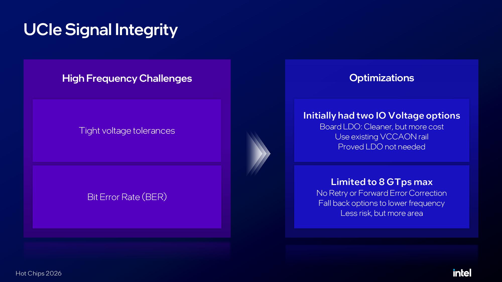
Choosing to leverage UCIe over an MCP design shaped the Wildcat Lake we have today, setting a roadmap for where Intel could cut compute to save cost and in areas where it would need to optimize to fit the necessary communication channels for the two chiplets.
UCIe integration in Intel Wildcat Lake
As Hacking explained during his presentation, budget parts usually involve an N-1 design. You leverage older IP, trim around the edges to improve the economics of yields, and repackage it as a mainstream part. Wildcat Lake is different in that regard. It's taking Intel's latest, most advanced, and most expensive IP for compute and applying it to the budget domain.
(Image credit: Intel)
With 18A at the center of the compute and ISMC's N6 handling the I/O die, Intel decided to make an MCP, which comes with some considerations. Advanced packaging allows designers to spend less die space on interconnects and use less power. With UCIe, Wildcat Lake's interconnect is 70% larger than that on Panther Lake, and even then, Intel says the change was worth it from a cost perspective.
(Image credit: Intel)
Outside of space, power was the primary concern with using UCIe. Battery life, especially for a budget part meant to handle lighter workloads, is extremely important, and UCIe brings increased power demands. UCIe die-to-die is packetized, which led to a challenging design point, particularly around the display.
Intel says that idle systems without panel self-refresh were the "biggest power concern," as display signals need to cross the UCIe connection. To address the issue, Intel says it built a buffer to hold panel refreshes while the system was idle. This buffer is before the UCIe link, and it serves as an additional output buffer alongside the typical display buffer between the memory controller and display engine.
(Image credit: Intel)
Without a base die for interconnect communication, UCIe also represents a large increase in die area. Intel trimmed a lot on both the compute and I/O dies to account for UCIe.
(Image credit: Intel)
On the compute die, Intel trimmed down everything. Four Xe cores dropped to two, and without a dedicated ray tracing accelerator, the NPU went from three tiles to a single tile, and the memory subsystem was downgraded to a 64-bit bus, with lower maximum speeds and lower capacity. As mentioned, there were a lot of cuts in the display engine, which was a primary concern for die space and power.
Intel uses three display pipelines instead of four, opting for HBR3 as opposed to the massive bandwidth offered with UHBR20. That still provides 4K60 and can drive three external displays, which is plenty for a device in the class that Wildcat Lake is targeting. Trimming down the compute die allowed Intel to claw back 38% of its die space.
(Image credit: Intel)
On the I/O die, Intel claimed back 15% die area by removing the camera PHY, reducing PCIe and USB support, and slimming down the audio engine. The camera was completely removed, placing the onus on OEMs to integrate their own controllers.
(Image credit: Intel)
UCIe 3.0 is capable of up to a data rate of 64 GT/s, but Intel capped the transfer rate in Wildcat Lake at 8 GT/s. That still allowed Wildcat Lake to support mainstream PCIe 4 SSDs and 4K60 external displays, but running at a lower data rate reduces bit-rate errors and therefore allowed Intel to remove some bit-correction systems.
Reducing the cost of Wildcat Lake
(Image credit: Intel)
Cutting down the compute and I/O dies saves money, but there are several other considerations when talking about the cost of a mobile SoC like Wildcat Lake. The economics need to work in the final product, which Intel touched on in its Hot Chips presentation, both from the perspective of the total bill of materials for OEMs and the yield/loss rate.
(Image credit: Intel)
The big factor in cost savings was the elimination of the base die, which not only reduces raw material costs but also comes with the yield upside, without advanced packaging.
(Image credit: Intel)
As usual, Intel bins Wildcat Lake into different SKUs, though it was careful to only attempt recovery where it could. For instance, it could package a single working P-core as a Core 3 304 instead of a 320. However, it didn't attempt recovery in areas that would compromise key design points of Wildcat Lake.
For instance, it didn't attempt recovery on LPE clusters and I/O, as they're critical components of Wildcat Lake. The goal, according to Intel, was to create a stack that customers actually wanted to buy while trying to maximize yields where possible.
(Image credit: Intel)
Intel also considered the full bill of materials for Wildcat Lake. Intel integrated Wi-Fi 7 and a USB PD controller, cutting costs for OEMs to integrate their own controllers. Perhaps the biggest point of savings was in memory, using a much slimmer bus and a 6-layer PCB as opposed to eight layers. Extending off the chart above is Project Firefly, Intel's initiative to leverage the mobile supply chain for budget laptops.
Interestingly, Intel also included an area that led to higher cost but met the design goals of Wildcat Lake, that being a dedicated power rail for the LPE cluster. The "low-power island," as Intel calls its LPE cluster, is critical to Wildcat Lake considering every SKU comes with only one or two P-cores. That dedicated power rail allows the vast majority of lightweight workloads to run on the LPE cluster and earn back battery life.
Wildcat Lake is one of the more interesting consumer launches we've seen in the past year. There's the MacBook Neo and Snapdragon C competing in the same space, but both use mobile SoCs in the traditional N-1 design point for budget platforms. Wildcat Lake is different, based on Intel's latest node, and leveraging newer open standards to achieve a lower price. That's why it won a Tom's Hardware innovation award for 2026, after all.
Full Intel Wildcat Lake Hot Chips 2026 presentation
Apple has today unveiled its next-generation M6 Apple silicon chip, as well as a powerful M5 Ultra. The new chips will debut in new versions of its Mac Mini and Mac Studio, respectively, available to pre-order from today.
The M6 is Apple's first chip on a 2-nanometer process, utilizing a 12-core CPU with two super cores, four performance cores, and six efficiency cores. The chip also features a 12-core GPU and a 12-core GPU featuring neural accelerators, alongside a "Dual 16-core Neural Engine." The top version of the chip has 170GB/s of memory bandwidth.
That dual 16-core neural engine means that there are indeed two neural engines. There's a connection between the engines, allowing them to run one model quickly across both, or two separate models independently.
The M5 Ultra is Apple's first chip using its UltraFusion technology to form a quad-die architecture (The M5 Max chips it is connecting both used two dies). The chip goes up to 36 cores on the CPU and up to 80 cores on the GPU, with 1.2TB/S of unified memory bandwidth, which Apple says is 50% higher than the M3 Ultra. Apple also claims the 36-core CPU with 12 super cores and 25 performance cores will offer "up to 1.25x higher single-threaded performance and up to 1.3x higher multithreaded performance than M3 Ultra."
The M5 Ultra has a 32-core neural engine, but this is different from the dual 16-core neural engine on the M6. Because the M5 Ultra uses a pair of M5 Max chips over UltraFusion, the 32 cores across the dies to run two models in parallel for increased performance.
Both M6 and M5 Ultra feature GPUs with neural accelerators and their fastest cores, marking a leap forward for Apple's graphics processors when it comes to AI.
Apple users who have been maxxing out previous versions of the Mac Mini will be capped at 32GB of memory on the Mac Mini with M6, like a choice the company made due to the component shortage that has been affecting the entire industry. If you want 64GB like the M4 Pro, you'll need the M5 Pro model. But the M5 Ultra in the Mac Studio won't have that problem, with Apple offering up to 512GB of unified memory on that chip.
M6 also features updates to hardware-accelerated ray tracing, dynamic caching, and the shader core, which the company claims will allow for faster rendering and higher frame rates in games.
Mac Mini and Mac Studio
The new Mac Mini and Mac Studio aren't seeing any design changes, though there are substantial internal changes. Both systems are available for pre-order today, but won't arrive to customers and in retail stores until September 22.
(Image credit: Apple)
Besides the M6 version of the Mac Mini, there will also be versions with M5 Pro. Both models will be bumped to Wi-FI 7 and Bluetooth 6, as well as 2.5Gb Ethernet (up from 1Gb), with a 10Gb option available as an upgrade. The Mac Mini also supports genlock via USB-C, synchronizing displays and cameras to prevent video drift during broadcasts.
For those working with AI, Thunderbolt 5 on the M5 Pro Mac Mini will allow customers to run clusters for on-device models.
The Mac Mini with M6 will start at $899, while the M5 Pro option will begin at $1,699 (each drops $100 for education pricing). Given that the Mac Mini with M4 started at $599, it's seeing substantial price hikes here.
(Image credit: Apple)
The Mac Studio will come with M5 Max or the new M5 Ultra chip, and Apple is positioning it for on-device AI. It will now offer up to six Thunderbolt 5 ports with support for as many as eight displays. Like the Mac Mini, it's also getting Wi-Fi 7 and Bluetooth 6 with Apple's N1 chip, which debuted in the iPhone 17 lineup. Like the Mac Mini, the Mac Studio also supports genlock for perfectly synced video.
The Mac Studio with M5 Max will start at $2,499 ($2,299 with an education discount), and the M4 Ultra model will start at an eye-watering $5,499 ($5,099 with an education discount).
Both systems will be compatible with macOS 27 Golden Gate, including Siri AI and refinements to the Liquid Glass design introduced in macOS 26 Tahoe.
Nvidia has spent the last several months providing key disclosures about its next-gen Vera CPU for agentic data centers, which it continued at Hot Chips 2026. Although we've already learned a lot about Vera, how it compares to AMD's next-gen Venice CPUs, and the inner workings of the Olympus core, Nvidia provided a bit more color at Hot Chips on spatial multithreading, the memory subsystem, and what types of workloads it's targeting with Vera.
As a quick refresher, Vera is the first CPU with a custom Nvidia core, following up on Grace, which used a stock Arm design. It's shipping as a single, 88-core SKU, and it has some key design differences compared to Nvidia's x86 competition, most notably a multi-threading implementation that Nvidia calls spatial multi-threading, an LPDDR5X memory subsystem, and a monolithic compute die rather than using compute chiplets.
Nvidia says it's designed Vera specifically for agentic AI workloads, a category that's still being defined in terms of performance benchmarking. Many CPU-intensive tasks serve as proxies for agentic workloads (i.e., code compilation), though measuring performance across a full agentic chain is complex and inconsistent. Nvidia, in its own slides (see the end of this article), calls agentic AI the "most complex computing workload in history," after all.
Nvidia provided an example of a headless browser to show the benefits of Vera, using optimized code to mimic how an agent would use a browser. Compared to the 96-core EPYC 9655P, Nvidia says Vera runs 24% faster as browser instances scale.
(Image credit: Nvidia)
This slide is a good demonstration of the complexities in measuring traditional workloads and applying that performance to agentic workflows. Agents will often fetch websites for information, but there are several layers where agents can trim back compared to humans; in this case, agents can run through a browsing workflow 4.5x faster by cutting things like GUI rendering, fonts, media decoding, and more.
(Image credit: Nvidia)
Another touchstone for agentic performance is code compilation, as agents seek out software to compile on the system. This might be the most direct benchmark of agentic AI performance with current workflows right now. Though, as previously mentioned, agentic chains are long, complex, and involve several different workloads.
Once again, compared to the 96-core EPYC 9655P, Nvidia claims Vera can compile the Linux kernel 22% faster with a native AArch64 target, and 14% faster when cross-compiling for x86.
Nvidia's big cores for agentic AI — another look at Olympus and how it fits into Vera
Nvidia reiterated the importance of the large cores inside Vera, including the large BPU, neural branch predictor, and 10-wide decode. Nvidia has previously disclosed the Olympus core architecture, which you can read about in our Vera deep dive. Broadly speaking, however, it's a wide core optimized for high single-core throughput.
One of the more interesting design points of Vera is spatial multi-threading, which Nvidia described in more detail during its Hot Chips 2026. In short, Nvidia separates core resources on two pipelines, though data and cache can move between threads as needed. To demonstrate the benefit, Nvidia shared the results from SPEC CPU 2017 intrate that you can see below.
(Image credit: Nvidia)
This shows the "noisy neighbor" effect. Nvidia measured single-core performance and then measured the same workload with another thread active. Nvidia's data shows that Vera is less concerned with the neighboring thread, whereas a "traditional CPU" sees a larger slowdown. Nvidia didn't clarify which CPU it's comparing Vera to here, however.
Nvidia's slide does a good job illustrating, but it's worth noting the difference compared to traditional SMT nonetheless. With traditional SMT, resources are time-sliced between threads, leading to gaps between BP and decode, as illustrated in the slide. With spatial multithreading in Vera, threads are still fighting for resources within the core. However, spatial multithreading allows Nvidia to deal with the demand of neighboring threads in a deterministic way, leading to a more consistent downturn in per-core performance when the second thread is working.
Nvidia's second-gen Scalable Coherency Fabric (SCF) moves data across the die. Nvidia didn't provide any new disclosures around SCF at Hot Chips, but you can see how the fabric is laid out in the slide below. Centralized Coherency Switch Nodes (CSNs) connect the cores to pools of L3 cache totaling 164 MB and the broader memory subsystem.
(Image credit: Nvidia)
At a system level, one of the more interesting choices Nvidia made was to use LPDDR5X as opposed to traditional RDIMMs, a choice that it was only able to make due to the serviceable SOCAMM2 design. Nvidia includes eight SOCAMM2 slots per Vera CPU on a board, offering up to 1.5 TB of capacity with 1.2 TB/s of bandwidth.
(Image credit: Nvidia)
LPDDR5X can deliver transfer rates higher than DDR5 RDIMMs, at least compared to single-rank DIMMs. However, it seems the driving force behind LPDDR5X wasn't performance but rather power consumption. One of the pillars of Vera, according to Nvidia's Hot Chips presentation, was to deliver a CPU for power-limited data centers. Micron says its LPDDR5X consumes about a third of the power compared to a traditional RDIMM.
(Image credit: Nvidia)
Nvidia demonstrated that point a little differently, using bandwidth per watt as a point of comparison between the LPDDR5X system in Vera and traditional RDIMMs. This illustration does the job, though it could be a bit misleading, measuring power draw against peak bandwidth.
Nvidia tells us that a fully loaded memory system with Vera consumes between 30W and 40W, with 1.5 TB at 9600 MT/s. Power demands for RDIMMs vary wildly depending on capacity, channels, and transfer rate, though power consumption can easily climb over 100W depending on the configuration.
Although Nvidia has deployed Grace in the data center — to the tune of "hundreds of thousands" of standalone servers, apparently — Vera represents Nvidia's first big push to gobble up market share in the expanding agentic CPU market. It's highly targeted, as evidenced by the fact that Nvidia is only delivering a single 88-core SKU, and it's already being put to use in large-scale deployments, with Nvidia announcing yesterday a deployment of Vera at SpaceXAI.
(Image credit: Nvidia)
Nvidia has shared the slide above before, which it once again showed at Hot Chips 2026. It's normalizing per-core performance in SPEC CPU 2026 against the AMD EPYC 9755. The core differences explain the big disparity in numbers; in reality, Vera led in overall score by 3%. Regardless, this is the slide Nvidia is using to pitch Vera, claiming it offers a big improvement in the workloads that are most relevant for agentic AI.
The most formidable opponent for Vera isn't Turin, however. It's Venice, which AMD launched in June, and Diamond Rapids, which Intel detailed just moments after Nvidia left the stage. Vera has a lot of interesting talking points already, but it'll be interesting to watch how Nvidia scales (or doesn't scale) its data center CPU business over the next few generations. Perhaps we'll see the firm double down on these agentic workflows, or maybe concessions and product segmentation to appeal to hyperscalers. Time will tell.
After teasing the chips earlier this year, Intel has provided some details on its next-gen Xeon 7, codenamed Diamond Rapids, CPUs. Featuring up to 256 P-cores and 1.28 GB of last-level cache, the new range of CPUs is set to release in the data center in 2027. The range brings forth several advancements we've expected on Intel's roadmap, including the enhanced 18A-P process, UCIe interconnects, AVX 10.2, and Intel's new "fan-out" fabric.
Intel didn't detail the core architecture (known as Panther Cove) in Diamond Rapids during its Hot Chips 2026 presentation, so we'll likely have at least one more technical deep dive on Diamond Rapids before it arrives, and possibly more. Although there are still questions about Panther Cove, Intel shared a technical breakdown of how Diamond Rapids chips are built more broadly, including a look at the compute tiles and how they come together across the chip.
Intel calls the compute tiles Compute Building Blocks, or CBBs, and they hold the core chiplet stacked on top of the base tile that holds the LLC. Each core chiplet can hold up to 16 cores, and based on the scaled-up Diamond Rapids SoC, up to four of those chiplets can live in a CBB. Each chiplet connects to the base tile with a 3D Xbar. A full Diamond Rapids SoC includes four base tiles built on Intel 3-T, two fabric hub tiles built on Intel 3, and 16 core chiplets built on Intel 18A-P.
Bringing everything together are two advanced packaging techniques. Intel is once again using its own Foveros Direct 3D to bond the compute tiles to the base tiles, as seen with Xeon 6+ 'Clearwater Forest' CPUs. Intel is using UCIe-S to connect the fabric hub tiles to the cores via a copper connection. Notably, Intel isn't using its own Embedded Multi-die Interconnect Bridge (EMIB) that it's broadly deployed in past products.
Intel Xeon 7 'Diamond Rapids' compute chiplet
(Image credit: Intel)
Diamond Rapids is built with four Compute Building Blocks, each of which includes four core chiplets that house 16 P-cores each. The cores have access to private L2 within each chiplet, and they share an L3 cache located on the base tile. The chiplets are connected to the base tile with a 3D crossbar, packaged with Foveros Direct 3D.
Within each CBB, there's 3D packaging, but Intel leverages 2D communication via a UCIe-S interconnect to connect the CBBs to two centralized fabric hubs, allowing the cores (and caches) to communicate with each other. Although there are two fabric hubs, each of the CBBs is connected to both fabric hubs, so communication routes are clear across the chip.
(Image credit: Intel)
Compared to Granite Rapids, Intel has quite literally flipped the layout, centralizing memory and I/O while pushing the cores out to the edges of the chip. It's much closer to a layout we'd expect to see from AMD.
Thermal improvements will likely follow. With the highest-clocked and hottest components pushed out to the edges, there's much less concern for hot spots in the middle of the chip, as is the case with Granite Rapids-AP, where the cores are at the center.
Intel is using its latest enhanced 18A-P node for the compute die, which is said to increase performance by 9% compared to 18A at peak performance, or operate at 18% lower power with iso-performance. Intel announced in June that 18A-P had entered risk production.
Diamond Rapids comes with 16-channel memory, supporting up to 8,000 MT/s with DDR5 and up to 12,800 MT/s with MRDIMMs. Although Intel bumped memory speeds with Xeon 6+ 'Clearwater Forest,' we're now seeing fast DDR5 support on a P-core Xeon, and with an expansion to 16 channels (Granite Rapids topped out at 12 channels).
Intel centralizes all of the hardware for memory and I/O communication in the middle of the chip across two tiles (the fabric hubs), and each CBB can communicate with both fabric hubs.
(Image credit: Intel)
Double-clicking into the diagram at the top of this section, you can see the layout of the I/O system above. Across the chip, Intel supports 128 lanes of PCIe 6.0, CXL 3.0, UPI 3, or some combination thereof, courtesy of the flexible I/O subsystem. Intel also includes four PCIe 4.0 lanes (a total of eight per CPU) for platform use.
The I/O fabric also includes complexes for the various accelerators on-chip in Diamond Rapids, including Intel QuickAssist Technology (QAT) and In-Memory Analytics Accelerator (IAA).
(Image credit: Intel)
In the memory fabric, you can see the standard flow through the DDR PHY into the memory controller, but Intel includes some special sauce at the end of the chain, notably an on-die snoop filter. A snoop filter is a directory to maintain cache coherency, and moving it onto the CPU removes directory storage and cache coherency tasks from the memory.
Interestingly, Intel isn't leveraging its advanced EMIB packaging to connect the fabric hubs to the CBBs. Instead, Intel is using a standard UCIe-S connection through copper in the substrate. Intel says that UCIe-S offered a "low-latency uniform connection to all of the memory hubs" that "made the most sense for Diamond Rapids."
(Image credit: Intel)
There were a handful of questions around UCIe-S versus an advanced packaging technique, UCIe-A. Intel says the choice mainly came down to distance, with UCIe-A requiring multiple "hops" depending on the distance. UCIe-S provides uniform access across longer distances, enabling lower latencies across the entire chip.
Intel Advanced Performance Extensions and AVX 10.2 support in 'Diamond Rapids'
(Image credit: Intel)
Although it's more of a footnote in the headline reveals about Diamond Rapids, the next-gen Xeon CPUs mark an important milestone in Intel's journey with AVX-512 and Intel's Advanced Performance Extensions, or APX, which has been described as a modernization of the x86 ISA. Both were described in 2023, and now they're showing up in Diamond Rapids.
First, AVX. Expectedly, Diamond Rapids marks the move to AVX 10.2, which is supported on both P-cores and E-cores (AVX 10.1 only worked on P-cores). AVX 10.1 served as a transition step off of AVX-512 and only supported 512-bit vector instructions. AVX 10.2 supports converged 256-bit vectors, enabling execution on both P-cores and E-cores.
Diamond Rapids also supports Intel's APX. APX doubles the number of general-purpose registers from 16 to 32 with new encoding for registers 16 through 31. Intel says software will see a performance improvement when recompiled with APX, and without source code changes. We heard about APX support in Panther Cove nearly two years ago for the first time.
APX requires 10% fewer loads and 20% fewer stores in memory, according to Intel, and includes some key instruction updates like condition load and store. It doesn't require a code change, either, with full compatibility with previous code bases.
Between AVX 10.2, AMX, centralized I/O and memory communication, and 18A-P, Diamond Rapids brings forth a lot of innovation that Intel has been talking about for a long time. Whether it's too little, too late remains to be seen with the missteps around Granite Rapids.
Given the explosion of CPU demand for agentic workloads, Intel has a competitive part here that, at least, supports the latest updates to the x86 ISA and borrows a lot of key design points from AMD's evolution with EPYC. Intel has continued to double down on Coral Rapids; however, the generation that will follow Diamond Rapids will reintroduce SMT to Xeon.
Full Intel Xeon Diamond Rapids Hot Chips 2026 presentation
 登录
登录