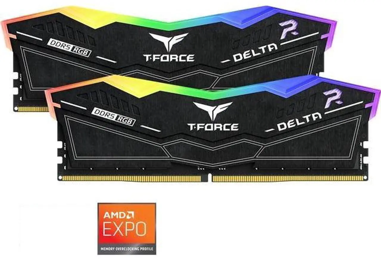
We're seeing 32GB DDR5 RAM prices regularly push above $400 now. That's just where the market is, and as unfair as it might seem, the world is still turning, and people still need memory for their PC upgrades. Luckily, this TeamGroup T-Force Delta RAM deal drops the price to $389.99 at Newegg, as long as you use the coupon code LUYRF228 at checkout.
Deals like this continue to be the best way to pick up new RAM as the ongoing global DRAM shortage, caused by the AI boom, rolls on. We're not going to see lower prices for RAM or SSDs any time soon. Deals like this aren't ground-breaking, and we're nowhere near record lows, but they're the best prices in a difficult market. Sans a time machine, or going second-hand, you won't find better pricing today than this.
As for this particular RAM kit, it's a good option for a mid-tier build. It's DDR5-5200, meaning speeds of 5,200 MT/s. That isn't the fastest RAM on the market, by any means, but it's certainly an upgrade over older DDR4 modules, which would usually see speeds of around 3,600 MT/s at best.
use coupon code LUYRF228 for $40 off
T-Force Delta RGB 32GB (2 x 16GB) DDR5-5200: was $429.99 now $389.99 This RGB kit from Team Group unlocks 32GB of DDR5 memory for your gaming PC or workstation rig. CAS and memory timings of 40-40-40-76, with speeds of 5,200 MT/s, mean this isn't the fastest memory out there, but it's currently the cheapest 32GB DDR5 kit you can buy.View Deal
You're getting two 16GB DDR5 modules here, with CAS and memory timings of 40-40-40-76. This is perfectly fine memory for workstation and gaming use, with built-in RGB lighting to spice up your build. Yes, it won't be the fastest you've used. If you need to max out a build with the best speeds and lowest latency, you'll need to look for higher-end DDR5 memory instead.
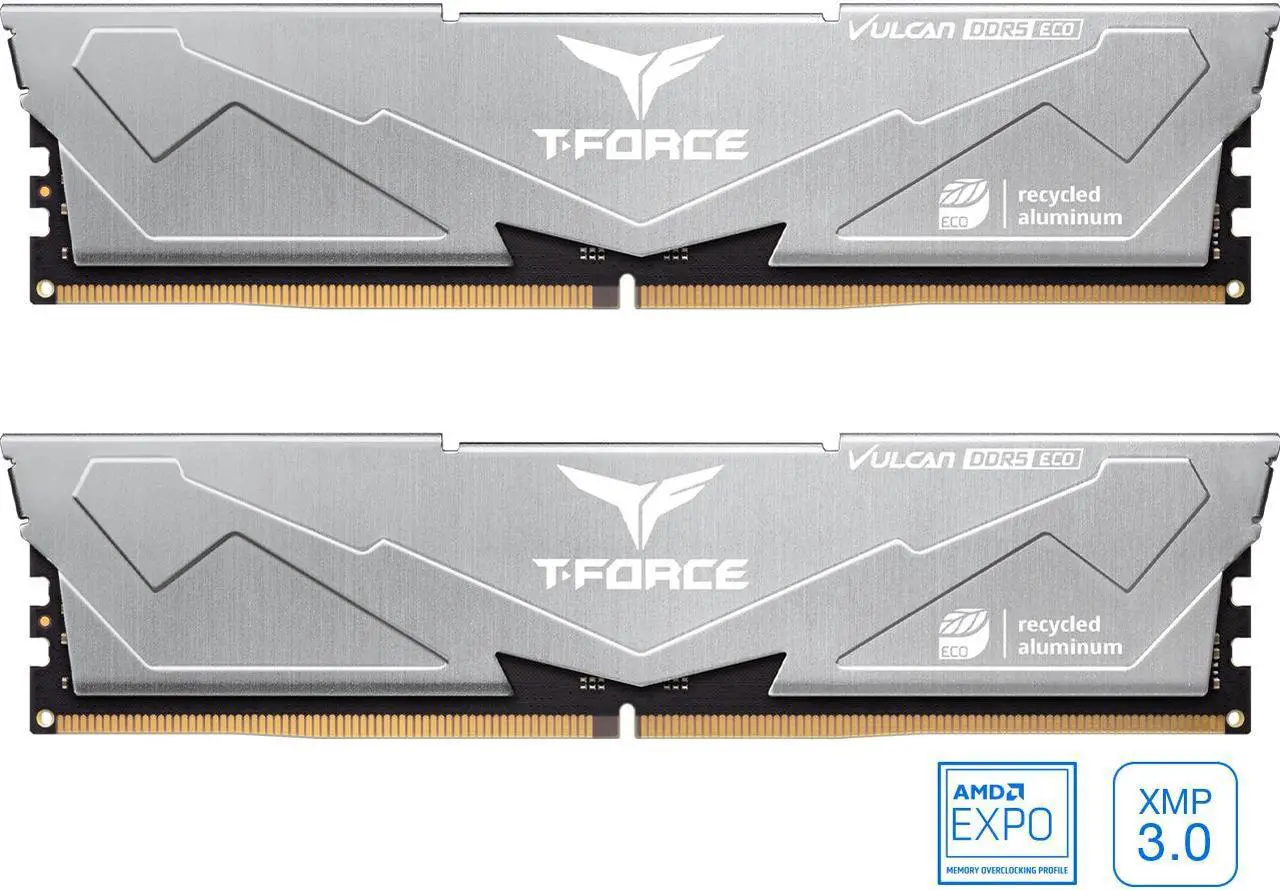
Luckily, you have options there. The next best option with faster speeds is this alternative kit, also from Team Group, for $415.99. The Team Group T-Force Vulcan has CAS and memory timings of 38-46-46-84, with speeds of 6,400 MT/s. Much faster, so ideal for a higher-end rig, but it lacks the RGB lighting. That might be a trade-off you're willing to accept if you've got the extra $27.
T-Force Vulcan Eco 32GB (2 x 16GB) DDR5-6400: $415.99 The next, best 32GB DDR5 RAM kit, also from Team Group, with much faster speeds of 6,400 MT/s. CAS and memory timings are 38-46-46-84. Probably the better option, if your budget can stretch to get it.View Deal
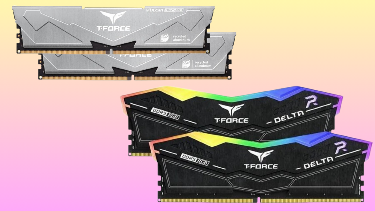
Honestly? The best option here, if you do have the extra cash, is the T-Force Vulcan for $415.99. It's faster, only slightly more expensive, and it's still a bargain compared to rival kits that can go as high as $600 or $700 at the moment. That said, a new PC build or upgrade on a budget requires a few compromises, and unless you're pushing your PC to its limits, the Team Group T-Force Delta RAM kit for $389.99 is a solid option.
Either choice is a deal worth considering in this awfully expensive market that PC builders face at the moment. AI isn't going anywhere, and we're probably going to see prices this high, if not higher, for some time. Deals like these, even if they aren't world-beating, are still the best way to get RAM at the moment.
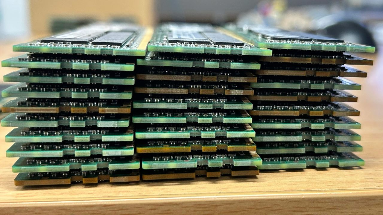
A computing enthusiast has shared images of a fat stack of DDR4 RAM sticks that they found at home. VastOption8705 told other tech fans on Reddit that they “found 10k worth of RAM sitting in my garage.” We count 30 sticks of DDR4-2666, and three sticks shown separately are all 64GB modules. If they are all 64GB modules, that number of sticks would add up to 1,920GB of RAM…
How did this huge amount of RAM end up in VastOption8705’s garage? The story goes that the Redditor was allowed to keep an old server from their workplace. Such 'generosity' isn’t unheard of, and it might have actually saved the company some recycling fees.
Is server DDR4 useful?
Numerous comments on the Reddit post jokingly pitch for RAM stick donations. But they might be barking up the wrong tree. Looking more closely at the sticks, where the labels are clearly readable, reveals that they are Samsung 64GB DDR4 ECC registered DIMMs (RDIMMs).
These kinds of RAM sticks are commonly used in servers built around Intel Xeon, AMD Epyc, or AMD Threadripper platforms. Sadly for their market value and the folks on Reddit hoping for some spare RAM, they aren’t consumer PC friendly. Even if you have a DDR4-supporting motherboard, these ECC RDIMMs will be both physically and electrically incompatible with your home creator/gaming PC.
Pricing and the Australia question
A quick poke around eBay U.S. listings shows that a single 64GB DDR4-2666 stick like those shown can be bought for between $350 and $425. So, we could roughly value the 30 sticks at $12,000 if a price of $400 per stick were achieved. The OP’s touted $10K valuation wasn’t far off. But if VastOption8705 lives in Australia, as they seem to, and guesstimated the value in Australian dollars, AU$10,000 currently equates to ~US$7,200 – quite low.
If you have spare RAM in your garage, don't share your address on public forums. The best I could find is a pair of 8GB DDR4 SO-DIMMs in my drawer. I also had some 30-pin SIMMs, SDRAM, PowerMac ROMs, and DDR3 modules probably worth just pennies, despite the RAMpocalypse.
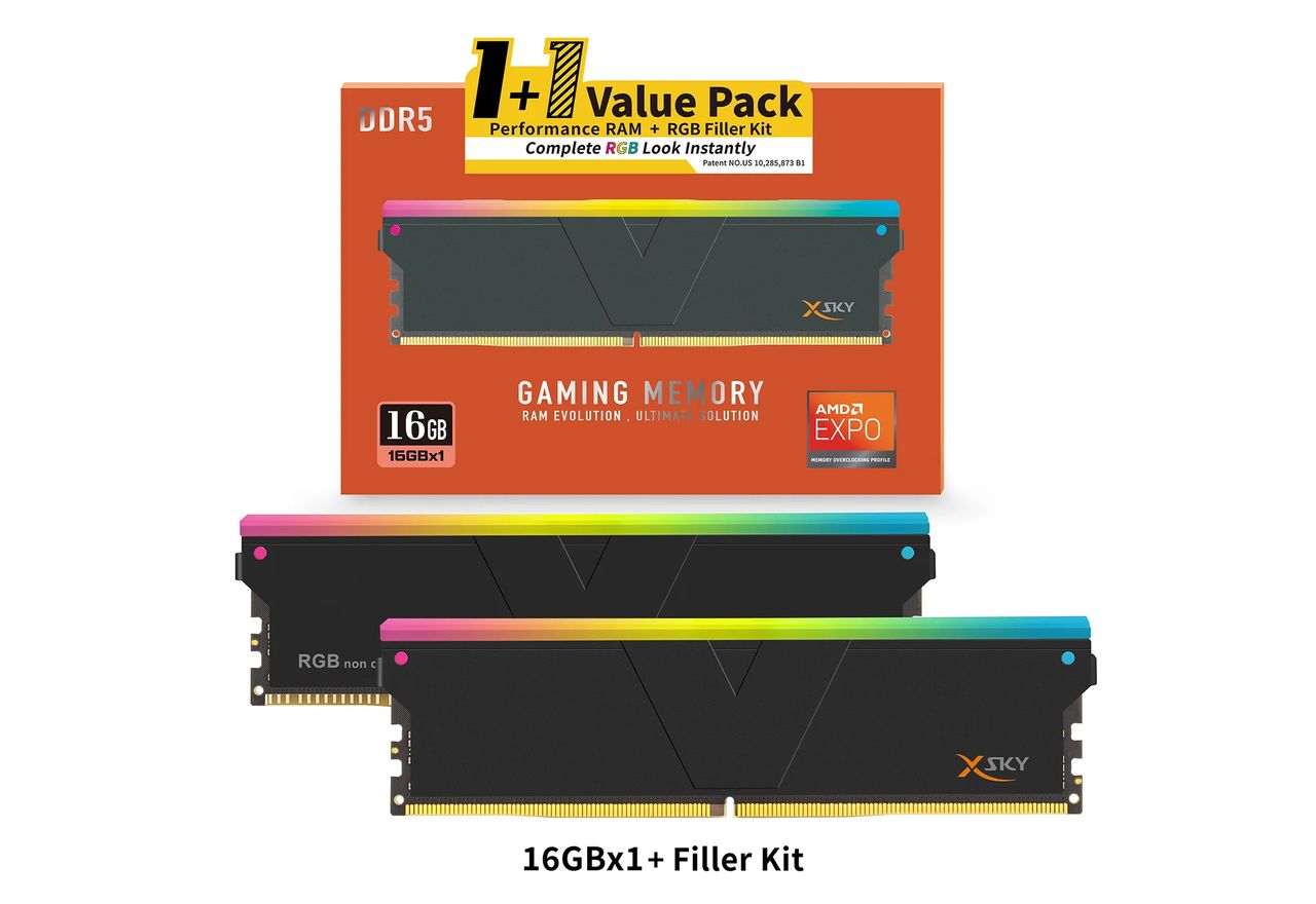
Earlier this year, V-Color announced its 1+1 DDR5 filler memory kits to help suspend disbelief and offer psychological salvation against rising memory prices. These kits mix real DDR5 sticks with dummy modules that don't actually have any RAM inside — just working RGB — to give you the illusion of a fully-slotted motherboard. Today, the kit is finally available to buy in the UK and Europe, with just the filler sticks on their own also listed for sale in North America.
V-Color has two different DDR5 products: Manta XSky and Manta XFinity, the latter being the higher-end model. The 1+1 kit is only available for the Manta XSky variant and only in the UK and Germany; not yet in the US. The 0GB kits (where both sticks are dummies) are available in both the Manta XSky and XFinity models across multiple regions. Pricing starts from $43 and goes up to almost $300, so let's break it all down.
In the UK, Overclockers currently has the 16GB 6,000 MT/s CL30 kit listed for 210 GBP, or $285, in black and white colorways. You get a single 16GB stick with those specs and a filler module to occupy two slots on your motherboard. There's a slightly more expensive 16GB 6,000 MT/s CL28 kit as well, selling for 219 GBP, or $297. Once again, you can choose either the black or white color, and you get 1 real stick of RAM and one filler.
In Europe, using Geizhals, we were only able to find one in-stock listing of the 16GB 6,000 MT/s CL28 kit for 330 Euros, or $384, in the black colorway. The same kit with CL30 speeds can be had for 220 Euros, or $256, but it's out of stock on CaseKing, the one Germany-based store in the entire EU with these products. We'll remind readers that there are no North America listings for V-Color's 1+1 DDR5 kits as of now.
But we did spot plenty of 0GB kits on Newegg and Amazon. These kits don't offer any real RAM whatsoever and are purely meant for decorative purposes. You can only use these if you already have working RAM in your system and two extra slots left to populate on your motherboard. Amazon has the Manta XFinity variant listed for $57 in either black or white, while Newegg is selling the Manta XSky model for $44 in white.
CaseKing in Germany is selling the Manta XSky filler kit for 50 Euros, or $58, but we weren't able to find any other listing across Europe. The prices for these kits across the world are not much higher than their regular, non-filler counterparts, so you might as well spring for these until the RAMpocalypse settles down. Just don't forget that you'd still be limited to single-channel memory with the 1+1 kits, which isn't that big of a deal when it comes to DDR5, especially if you have an X3D CPU.
The saga involving Chinese DRAM maker CXMT's alleged theft of Samsung's trade secrets is going strong. The South Korean court case already includes multiple convictions, two of which carry prison sentences for ex-Samsung engineers. The latest chapter is a doozy, though. Korean publication NoCut News spilled the chips on Project Hefei, a purported CXMT roadmap outlining long-term planning about said technology "acquisitions," personnel poaching, and production tape-out — all key pieces that may have directly led to CXMT's ascension to 10% of the global DRAM market.
According to leaked court documents, the prosecution says that Project Hefei was CXMT's entire DRAM development plan and was spearheaded by the firm's head of development (formerly Samsung's DRAM development lead), around August 2016 — not much longer after CXMT itself was created in June 2016.
In brief, the purported plan was to nab Samsung's Process Recipe Plan (PRP) by September 2016, poach key Samsung engineers by October 2016, have R&D complete in July 2017, and start making DRAM wafers by August 2018 at a rate of 10,000 a month. NoCut says the PRP dataset comprises 620 steps in DRAM manufacturing and includes data on equipment, consumables, and production methods.
The report states that in August 2016, CXMT first attempted to make wafers of 18nm chips by relying on the collective memories of the Samsung engineers it had hired away. Those recollections apparently proved insufficient, so after allegedly gaining illicit access to Samsung's PRP, CXMT prepared its own document in September 2016. The leaked data even included specific equipment suppliers and model numbers.
CXMT's "new" PRP was then handed out to key specialists, many of them ex-Samsung engineers, whom the prosecution says ought to have immediately recognized the data as originating from the Korean firm. The document apparently included notation and notes on process developments that were all unique to Samsung. A convicted ex-Samsung researcher with the surname Jeon, previously sentenced to 7 years in prison for manually copying parts of the PRP before leaving for CXMT, testified in this case as a witness.
The whole CXMT debacle has been playing out in South Korean courtrooms since January 2024 and is arguably far bigger than just "a company stole some tech from another." A decade ago, most of the DRAM market was taken by the Big Three: Samsung, Micron, and SK hynix. CXMT was created in June 2016 in Hefei (hence the project name), with a modest government investment of around $1.9 billion USD, allegedly withno R&D facilities whatsoever or any plan for research.
Going from zero facilities and institutional expertise to DRAM wafer production in little over two years would be an unprecedented feat, and presumably nigh impossible without the alleged IP theft; getting just the memory fab up and running usually takes two to four years, let alone any time for research. The firm claimed in 2019 that it designed its then-new 8 Gb DDR4 chips entirely in-house as a "leapfrog, independent" technology and began selling DRAM chips locally.
Then the AI locusts charged in and ate every chip on the planet. This demand resulted in explosive growth for CXMT, from an estimated 4% of the global DRAM market in Q2 2025 to around 10% in Q2 2016, marking the first time in over a decade that the Big Three held less than 90% of the pie.
Production capacity expanded to three 12" wafer fabrication facilities, expected to churn out a collective 350,000 wafers until the year is done — close to the same figure that Micron produces, of 375,000 to 385,000. CXMT is also planning to open a second fab in Beijing, aiming to produce over 600,000 wafers per month once it's online.
Furthermore, CXMT's gains aren't coming just from its DRAM market share. Revenue grew 716% in Q2 2026 alone, and its IPO on the Shanghai STAR Market in July 2026 saw its stock climb 466%, netting the firm a cool $8.6 billion USD and making it the most valuable chipmaker in the Chinese stock market.
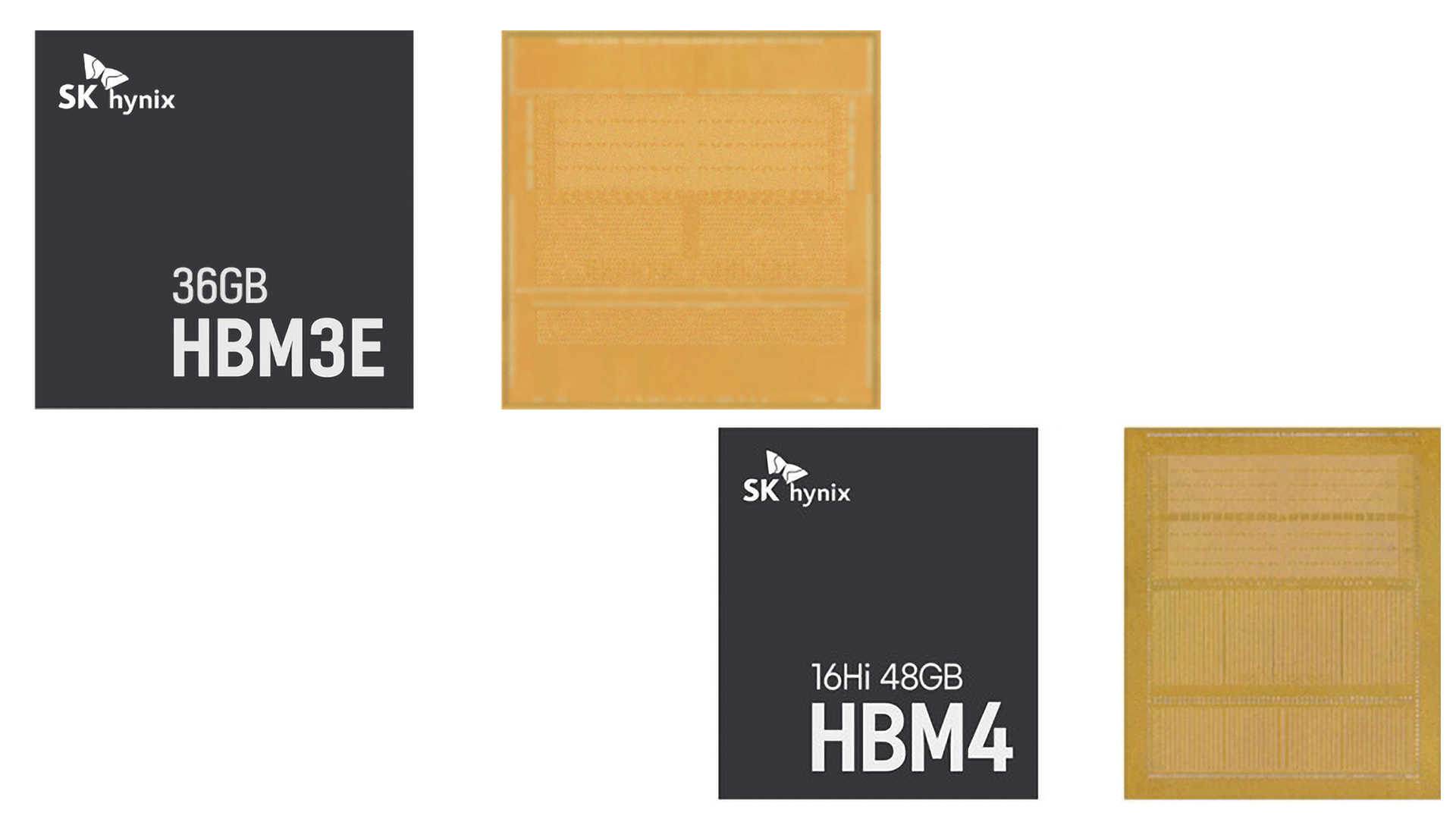
About 70% of that money is reportedly going towards further expansion of DRAM production, rather than pricier, more complicated HBM. However, the firm has supplied HBM3E samples to Alibaba's T-Head and Cambricon, even as Samsung and SK hynix enter HBM4 production.
As of the South Korean prosecution's last tally in December 2025, Samsung's damages due to CXMT's alleged machinations ascended to "at least tens of trillions of won." A back-of-the-envelope extrapolation, considering quite a while has passed, might suggest a figure in the range of ₩40 trillion, or $29.5 billion, and rising exponentially.
The lasting impact on the memory market and technology in general is going well beyond plain number descriptors, though. All things considered, if the allegations are true, then CXMT's machinations resulted in a geopolitical-scale economic event. Dr. Evil would be proud.
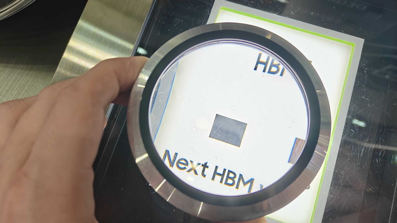
The goal of next-generation HBM5 memory specification is to double performance and increase power efficiency compared to HBM4E, Samsung announced at the 'Memory Executive Summit,' an event that precedes 'Semicon Taiwan 2026.' Considering that it is barely realistic to double the data transfer rate of HBM4E in just one generation, the comment made by Samsung may imply that HBM5 will double the number of interface pins to boost bandwidth.
The goal of HBM5, which is currently under development, is to double the performance and improve the performance per watt by 20% compared to the HBM4E generation, according to Choi Jang-seok, the head of the product planning team of the memory business department of Samsung Electronics DS division. Previously, Samsung announced that its HBM5 memory stacks will feature a heat path block (HPB), which will reduce thermal resistance by 20% and simplify cooling of HBM5 modules.
Doubling HBM5’s per-stack memory bandwidth would result in peak bandwidth of around 4 TB/s per stack already in 2028 – 2029. TSMC expects AI accelerators to get to 20 – 24 HBM5/HBM5E per package configurations by the end of the decade, which means that these systems-in-packages will get a whopping 80 TB/s – 96 TB of memory bandwidth just several years down the road.
Although both DRAM makers like Micron, Samsung, or SK hynix as well as developers of HBM controllers and PHYs like Cadence, Rambus, or Synopsys already offer HBM4/HBM4E controllers and interfaces rated for 16 GT/s data transfer rates, the official JEDEC transfer rate for HBM4E will be around 12 GT/s.
If Samsung expects HBM5 to deliver twice the bandwidth of HBM4E, the HBM5 specification must either double the per-pin data transfer rate from 12 GT/s to 24 GT/s, double the interface width from 2,048 to 4,096 bits, or combine a wider interface with a higher data transfer rate. Increasing HBM5 memory stack interface width to 4,096 bits has so far been envisioned by KAIST and Marvell; however, this is certainly not an even semi-official confirmation of the specification's target.
From a performance-per-watt perspective*, widening the interface is generally easier than doubling the per-pin signaling rate. Higher per-pin speeds require faster drivers, receivers, clocks, equalization, tighter timing margins, and a more sophisticated PHY since maintaining signaling integrity at speeds well beyond 20 GT/s is not easy. But while a wider HBM interface moves more bits in parallel at a lower speed per wire, going from 2,048 to 4,096 pins means twice as many TSV/I/O paths, drivers, receivers, bumps, more complicated routing, and extremely complicated base die. So while a 4,096 I/O at moderate speed is probably best for pJ/bit, the interface/package complexity gets so extreme that it may offset the gains. Furthermore, such a wide interface Perhaps a 3,072-bit interface combined with a moderate increase in data transfer rate would be a reasonable engineering compromise, though engineers involved in JEDEC’s decision-making process may think otherwise. In any case, for now, any discussion of HBM5 specifications remains speculative.
Nonetheless, the target to double the bandwidth of HBM4E (2 TB/s per stack) within one generation is clearly a very aggressive one.
*It should be noted that achieving a 20% higher energy efficiency can be achieved not only by increasing performance, but by improving DRAM process technology, optimizing base die, lowering TSV I/O voltages, architectural changes, or power management.
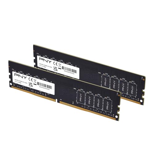
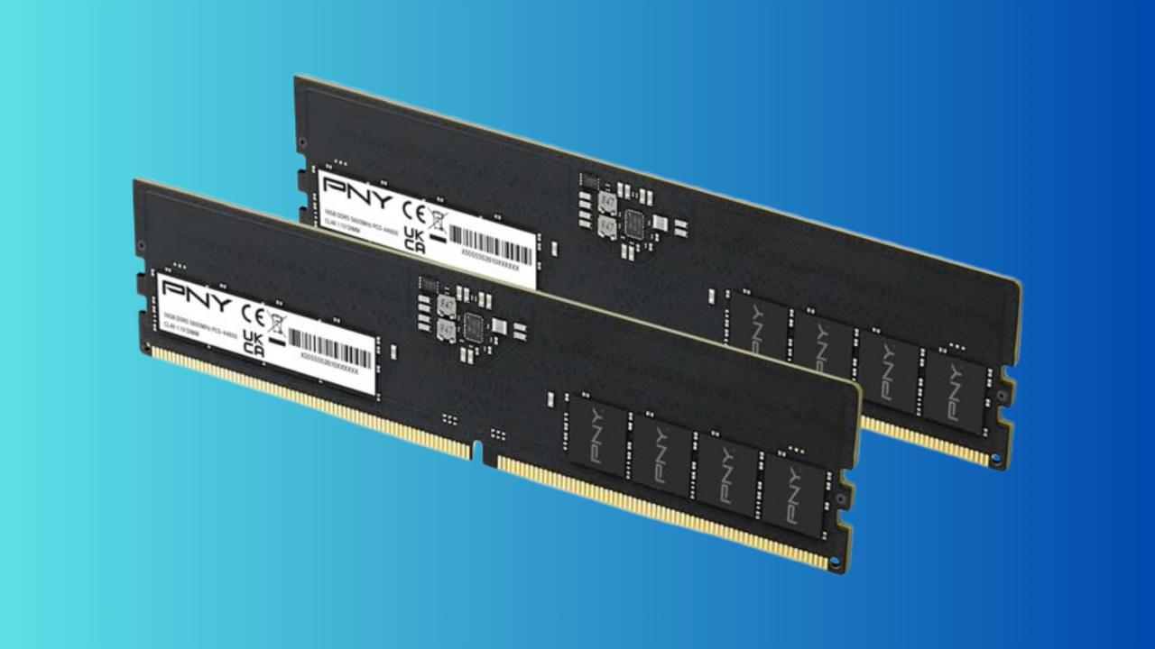
The RAMpocalypse means that, unfortunately, memory has become one of the most expensive parts in a new gaming PC build or upgrade. The ongoing global DRAM shortage means that you're going to need to pick up deals as they pop up. They're not ground-breaking deals or record lows, but they're the best prices in the current market. That's where this PNY DDR5 offer comes in, bringing the price of 32GB DDR5 down to just $399.99.
Believe it or not, this is where we're at with DDR5 RAM kits right now, and without a time machine (or buying second-hand), you're not going to find better pricing. This is the cheapest kit on sale at this spec and capacity, and after prices recently shot up past $400, it's a good offer to see it drop back below for the time being.
Our RAM price tracker shows how bad the market is for memory right now. You won't find a single option hitting below its record-low price floor, with many of the most popular models out of stock, too.
With this PNY kit, you're getting two 16GB DDR5 modules in this kit, capable of running at 5,600 MT/s, with CAS and memory timings of 46-46-46-90. This is high-performance RAM, suitable for gaming and workstation use. It isn't the fastest, but it'll do the job, as long as you're not looking to match the speeds (and higher prices) you'll find in higher-end DDR5 memory.
Unlike some of the RGB-packed options that gamers sometimes prefer, this PNY kit is pretty bare-bones as far as design goes. There's no RGB lighting at all, with just a black PCB finish and no heatspreaders. This is an install-and-forget kit that isn't meant to be flashy.
The $399.99 sale price for this PNY Performance DDR5 32GB memory is the real factor here: it's a price that simply can't be beaten right now. If you're building a new PC or upgrading your existing one, this PNY kit is a deal worth considering in the current market.
China's DRAM champion ChangXin Memory Technologies (CXMT) has started risk production of HBM3E memory, The Information reports. Although CXMT remains a generation behind the big three memory manufacturers, which are mass producing HBM4, it goes without saying that reaching the HBM3E milestone highlights the company's rapid technological progress.
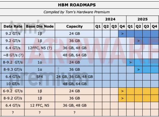
Specifications of CXMT's HBM3E products are unknown, though keeping in mind that we are dealing with risk production, specifications of actual HBM3E products from CXMT may differ from risk production samples. Meanwhile, general JEDEC specifications are well known: HBM3E modules feature a 1,024-bit-wide memory interface, supports data transfer rates up to 9.6 GT/s per pin, and can stack 8 or 12 memory devices. Depending on the exact speed bins, HBM3E can provide up to 1.228 TB/s of memory bandwidth.
Capacity of actual memory stacks depends on the number of DRAM dies used in that stack: HBM3E products can offer 24GB of capacity using an eight-die stack or 36GB using a 12-die stack when built with 24Gb DRAM devices.
Several Chinese developers of advanced processors are already evaluating CXMT's HBM3E with their processors, including Alibaba Group's T-Head and Cambricon Technologies, according to the report. If testing and qualification proceed as planned, these companies could begin using CXMT's HBM3E in commercial products as early as next year.
Since every HBM package requires multiple large DRAM dies, growing HBM output could consume considerable DRAM manufacturing capacity, which is when CXMT's aggressive capacity expansion will be useful.
CXMT's manufacturing of HBM3E is important for multiple reasons and arguably the HBM3E generation itself matters less than CXMT's ability to manufacture usable HBM at all.
Firstly, HBM is one of the critical components of modern AI accelerators, so if CXMT's HBM3E qualifies with processors from Cambricon, T-Head, and other Chinese designers, China becomes less dependent on Micron, Samsung, and SK hynix for building high-performance AI hardware.
Secondly, despite being a generation behind HBM4, HBM3E is still very capable memory and can provide several TB/s of bandwidth, sufficient for powerful AI accelerators. In fact, many Chinese developers of AI accelerators do not necessarily need HBM4/HBM4E to build useful AI systems.
Thirdly, HBM is substantially harder than making ordinary DRAM. CXMT needs not only competitive DRAM dies, but also high-yield stacking, through silicon vias (TSVs), very fine interconnects, thermal management, packaging, and testing. Reaching HBM3E risk production proves that China's memory ecosystem is advancing beyond simply manufacturing commodity DRAM.
Finally, there is also an important geopolitical angle. Export restrictions constrain China's access to advanced AI processors and HBM, so a combination of Chinese-designed accelerators, CXMT HBM3E, and advanced domestic packaging indicates that China becomes one step closer to semiconductor self-sufficiency.
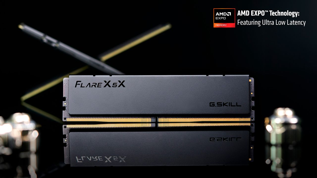
G.Skill, which makes some of the best RAM on the market, has announced the Flare X5X series of DDR5 memory kits. Like the Trident Z5 NeoX, the new Flare X5X leverages AMD's EXPO ULL (Ultra Low Latency) technology, which features optimized memory subtimings to maximize performance on Ryzen processors, especially those without 3D V-Cache.
G.Skill offers a plethora of different DDR5-6000 memory kits across its Trident, Ripjaws, and Flare lineups. It also offers variations that specifically cater to Intel and AMD processors. Historically, the Flare series targets AMD platforms.
The Flare X5X will initially launch at DDR5-6000, since many consider it the sweet spot for AMD's Ryzen chips. Like the other offerings, the Flare X5X debuts with a 32GB memory kit, made up of two 16GB memory modules.
As with any AMD EXPO ULL memory kit, it is difficult to tell the Flare X5X apart from the vanilla Flare X5 since we are not accustomed to listing specifications beyond the main memory timings. In the case of the Flare X5X, the memory kit has its timings configured to 36-36-36-96 at 1.35V, the same as the normal Flare X5 memory kit. The memory subtimings are tighter on the Flare X5X because of AMD EXPO ULL.
With memory timings of 36-36-36-96, the Flare X5X is not the best AMD EXPO ULL memory kit G.Skill offers. The company sells more optimized variants, including 26-36-36-32, 28-36-36-32, and 30-38-38-32 at 1.45V, 1.40V, and 1.35V, respectively. It is plausible that G.Skill will offer similar configurations for the Flare X5X down the line.
When AMD first announced it, the chipmaker confirmed that EXPO ULL memory kits would be priced similarly to regular EXPO memory kits. However, because of the memory shortage and leftover stock, the price difference was substantial. Pricing for AMD EXPO ULL memory kits has somewhat stabilized over the last few months, so the price tags are falling in line with what AMD anticipated.
G.Skill has not shared the pricing for the Flare X5X DDR5-6000 C36 32GB (2x16GB) memory kit. However, we should have a pretty good idea of what it will retail for by looking at G.Skill's other memory kits on the market. For instance, the Trident Z5 NeoX RGB DDR5-6000 C36, a less optimized version of the C30 version we have reviewed, sells for $10 more than the normal Trident Z5 RGB DDR5-6000 C36. In a perfect world, the Flare X5X DDR5-6000 C36 may sell for around $509.99, $10 above the standard Flare X5 DDR5-6000 C36.
G.Skill will roll out the Flare X5X series in phases so that availability will vary by region. It should not be long before we find the Flare X5X DDR5-6000 C36 memory kit at all major U.S. retailers.
ChangXin Memory Technologies (CXMT) has announced in a social media post that it has started mass production of LPDDR6 memory for a Xiaomi smartphone, Reuters reports. This is not entirely unexpected given the general LPDDR6 mass-production timeline, but the announcement is still surprising because two China-based companies are ahead of industry announcements. Yet, there are caveats.
LPDDR6 is perhaps the most substantial upgrade to the GDDR-class memory ever. Firstly, it uses PAM3 signaling, which encodes 3 bits of information across two symbols, compared with the NRZ signaling used by LPDDR5/LPDDR5X. Second, the data transfer rate increases to 43.2 GT/s. Third, the reduced I/O width from 32 bits to 24 bits requires rework at both the hardware and software levels.
Given the differences between LPDDR5 and LPDDR6, the most important factor here is not exactly LPDDR6 manufacturing, but a broader view.
On the one hand, CXMT reached mass production of LPDDR6 roughly at the same time as the established DRAM leaders, meaning it is on par with them, if not ahead. This marks a substantial change from earlier generations, when Chinese DRAM technology generally lagged considerably behind Samsung, SK hynix, and Micron.
On the other hand, reaching mass production does not necessarily mean that CXMT has achieved full technological or manufacturing parity with its larger rivals. The official announcement covers only one smartphone maker and one model, meaning CXMT's LPDD6 still has to pass validation for other handsets and other makers.
Still, the significance of CXMT's announcement is hard to understate. CXMT is no longer merely catching up by introducing a new memory generation years after its international competitors. With LPDDR6, CXMT is entering the market during the standard's initial commercialization, which means the technology gap between China's leading DRAM producer and the industry's established players has narrowed considerably.
Which brings us to the question of whether CXMT can maintain this pace. Developing a competitive LPDDR6 device is one thing, producing it at high yields and in sufficient volumes to supply major customers is another. For now, we are talking about a niche smartphone with memory operating at undisclosed performance.
If CXMT can mass-produce LPDDR6 for the whole market and manufacturers, we may well have seen the change of the industry leader. Yet, given one niche device, we certainly cannot say so for now.
China's leading DRAM producer ChangXin Memory Technologies (CXMT) has filed a lawsuit against the U.S. Department of Defense in an attempt to overturn its classification as a company linked to China's military, Reuters reports. CXMT claims that it has no connection to the Chinese People's Liberation Army, and argues that the Pentagon's decision lacks supporting evidence, violated due-process requirements, and has damaged both its business and reputation.
The Pentagon initially classified CXMT as a Chinese military company in January 2025, when Joe Biden was the president. The Trump administration subsequently maintained the designation when the Defense Department updated the list in June. CXMT says it spent more than a year supplying information to the Defense Department in an attempt to overturn the classification and remove itself from the list.
The company claims the DoD published a notice in February indicating that CXMT would be taken off the list but withdrew that notice later the same day without any explanation. In June, the Pentagon classified CXMT as 'directly affiliated with MIIT and indirectly affiliated with SASAC and MIIT.' MIIT is China's Ministry of Industry and Information Technology, whereas SASAC is the State-owned Assets Supervision and Administration Commission of the State Council, an organization that formally owns the government's stakes in non-financial state-owned enterprises.
While CXMT memory can certainly be found in systems used by the PLA or China's secret services, this does not automatically make CXMT a direct supplier to these entities and therefore does not prove that CXMT is a Chinese military company.
CXMT points out the Pentagon's original motivation to include the DRAM maker in its list was a remarkably weak-looking 'military grade' argument. According to the complaint, DoD's 2024 report said CXMT contributed to China's defense industrial base partly because its DRAM is dual-use and cited an advertisement describing CXMT products as 'military grade.' CXMT says that advertisement came from an unauthorized distributor, which later admitted the characterization was erroneous.
In addition, CXMT claims that its DRAM products conform to JEDEC commercial standards and lack the requirements imposed on Chinese military-grade semiconductor components involving areas such as temperature, packaging, testing, and military oversight. Also, it says that should its products be made in the U.S., they would be classified as for 'purely civilian uses' and that it 'does not hold any licenses to manufacture products for military use.'
Inclusion on the Pentagon's list of companies linked to the Chinese military can result in restrictions involving U.S. government contracts, something that CXMT barely seeks. But more importantly, it can affect a company's commercial relationships (as many companies do not want to be affiliated with companies linked to the Chinese military) and reputation. Indeed, CXMT claims that since January 2025 the designation has continuously hurt it commercially and reputationally, and that the lawsuit is intended to protect its business interests.
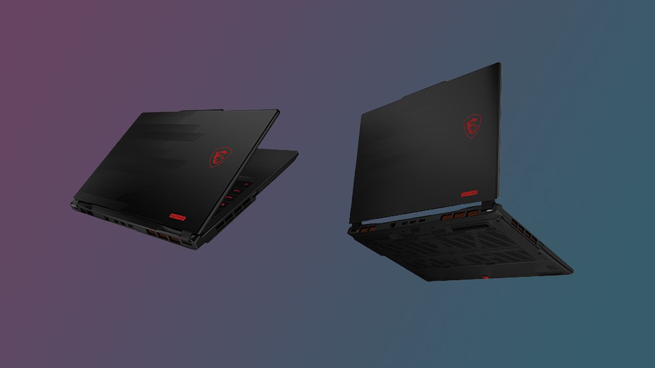
The ongoing DRAM crisis has led to a sharp increase in laptop prices, with manufacturers facing exponentially high component costs, particularly memory and SSDs. The situation has created a growing gap in the affordable gaming laptop segment, with most entry-level models becoming increasingly expensive. In its response, MSI has introduced the new Katana 15 HX C14 that features Intel’s 14th-gen Raptor Lake Refresh processors along with support for both DDR5 and DDR4-3200 memory.
Depending on the region, MSI will be offering the value-focused gaming laptop in two variants, featuring dual SO-DIMM slots with either DDR4 or DDR5 compatibility. For context, a 32GB (2x16GB) DDR4-3200 SO-DIMM memory kit can be purchased for around $200, while a DDR5-6000 kit goes for over $400. MSI did not specify the DDR4 capacity as standard, only that the laptop supports up to 96GB, which seems unlikely given no 48GB DDR4 SO-DIMMs exist.
Configurable with up to a 24-core Intel Core i9-14900HX processor, the laptop should offer plenty of CPU performance for demanding tasks besides gaming. It will be available with up to an Nvidia RTX 5070 laptop GPU offering support for the latest AI features, GDDR7 memory, DLSS 4.5, and real-time ray tracing. MSI claims that the Katana 15 HX C14 is tuned for up to 170W of combined CPU and GPU power, while the cooling system with dual fans, three heat pipes, and four exhaust outlets helps in sustained performance. There are also dual-PCIe Gen 4x4 M.2 slots, allowing gamers to add a separate SSD dedicated to their gaming library.
Display options include a 15.6-inch IPS panel available with either QHD (2560x1440) resolution that supports up to a 165 Hz refresh rate or FHD (1920x1080) resolution with up to a 144 Hz refresh rate. In terms of design, the laptop comes in a stealthy black finish with textured slash patterns inspired by traditional Japanese blades along with bright red logos. The chassis measures 22.9mm in terms of thickness and weighs 4.62 pounds, making it fairly compact for a 15-inch gaming notebook.
Other notable features include support for Wi-Fi 6E and Bluetooth 5.4, a 4-Zone RGB gaming keyboard with 1.7mm key travel, a 240W power adapter, USB Type-C with Power Delivery 3.0, a 60Whr battery, and DTS-enhanced dual 2W speakers. According to MSI, the new Katana 15 HX C14 will be available globally, although there's no pricing information at the moment.
Cloudflare says that it has freed up roughly 100TB of RAM across its global fleet without reconfiguring any physical RAM modules in its servers, and that it did so by redesigning how each DNS cache entry is laid out in memory. In a technical blog post, systems engineer Sebastiaan Neuteboom gave us an in-depth look at five Rust-level changes to Big Pineapple, the platform behind the 1.1.1.1 resolver, that shrank each cached entry from 953 bytes to 420 bytes and made the cache faster in the process, with insert throughput up 43% and lookup latency down 19%. The recovered memory matches the combined DDR5 in 130 of Cloudflare's 768GB Gen 13 servers, reclaimed in the face of server-grade DDR5 prices that are on track to double year over year.
Just one wasted byte per entry costs Cloudflare more than 250GB of fleet memory, which is a consequence of Big Pineapple holding more than “250 billion cached DNS entries at any given time.” The first of the five changes, replacing Rust's growable Vec and String containers with fixed-size boxed slices, saved over 15TB on its own by dropping capacity fields the data never uses once cached.
Further changes collapsed the three record lists in every DNS response into one buffer indexed by 2-byte offsets, and dropped owner names that duplicate the queried domain, rebuilding them at read time instead. The last change stores record data as length-prefixed raw wire-format bytes, ending an arrangement in which a 4-byte A record took up the same 144 bytes as the largest record type Cloudflare caches, the rarely seen NAPTR.
Packing record data contiguously also improved CPU cache locality, meaning that most record types now copy straight from the stored buffer into outgoing responses instead of being re-serialized field by field.
According to Cloudflare’s benchmarks in the technical blog, insert throughput is now 893,000 entries per second, up from 625,000, with lookup latency down from 828 to 670 nanoseconds. Over the rollout, which ran from mid-May to early July, p99 resident memory per instance fell from 9.3GB to 5.3GB.
The Gen 13 servers, which Cloudflare calls its most powerful yet, each carry 768GB of DDR5-6400. The company settled on that config back in March after pricing out a 1,152GB option and rejecting it partly because of high memory prices.
This DNS cache work is the second large memory-reclamation project Cloudflare has completed in the last year, following the FL2 rewrite of its request-handling layer in Rust last September. Efficiency has been driving the company’s hardware picks for years, including the switch to AMD's 96-core EPYC 9684X for its Gen 12 servers.
None of the liberated RAM will be cashed out as smaller memory configurations, though; Cloudflare plans to pour it back into larger DNS caches, which raise hit rates and cut the query traffic it sends upstream to authoritative servers.
High-bandwidth memory (HBM) is one of the key components of AI systems that is not currently assembled in the U.S., but this is going to change in 2029, when SK hynix initiates packaging of HBM memory modules at its facility in Indiana. This week, the company held a groundbreaking ceremony for its HBM production base in America and intends to start construction of the plant shortly.
SK hynix's HBM production site in West Lafayette, Indiana, will specialize in advanced packaging, testing, and R&D of HBM. The facility is set to cost the company around $4 billion, which highlights its advanced technology capabilities as well as vast capacity. The DRAM maker expects to open the cleanroom by October 2028 and begin volume production of next-generation HBM in the second half of 2029, which is about a year later than originally envisioned. Once commercial operations kick off, SK hynix expects the Indiana site to employ around 1,000 people.
Despite being described as an HBM production base, the Indiana site will not manufacture the DRAM wafers, but will package HBM stacks using DRAM wafers produced in South Korea and base dies produced in South Korea, Taiwan, or the U.S. Nonetheless, SK hynix intends to market the resulting devices as its first U.S.-made next-generation HBM products. Meanwhile, as custom HBM-class memory gains traction in the second half of the decade, assembling such stacks close to American customers may be particularly important both for SK hynix and its clients, as it enables SK hynix to shrink the feedback loop significantly.
In addition to building the advanced packaging and testing plant, SK hynix will also establish an Advanced Packaging R&D Testbed next to the manufacturing lines. The facility will enable SK hynix to work with customers, universities, and commercial partners on future packaging technologies, build prototypes, and quickly validate their performance and manufacturability in an actual production environment. In the era of customized HBM, such a facility could become a significant competitive advantage for SK hynix.
SK hynix also signed a memorandum of understanding with Purdue University to jointly research system integration and advanced packaging technologies, including HBM.
"The United States is the epicenter of AI innovation, bringing together premier customers, top-tier R&D capabilities, and partners and Indiana fab will become a gateway to deliver first Made in USA HBM products," said Kwak Noh-Jung, CEO of SK hynix. "We will expand our investments and collaboration in the U.S., grow together, and become the most trusted partner in shaping the future of AI in America."
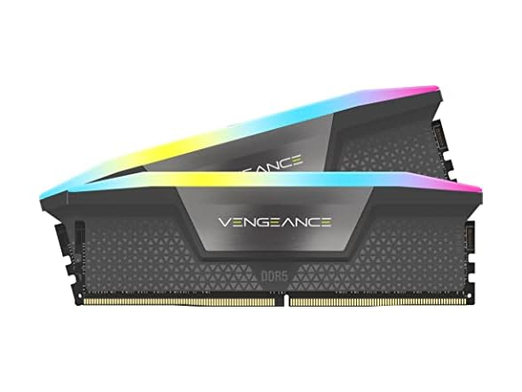
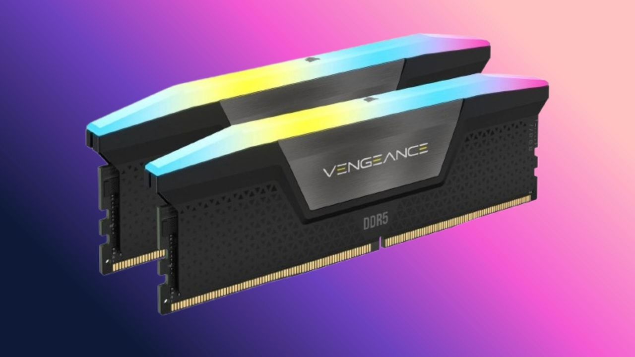
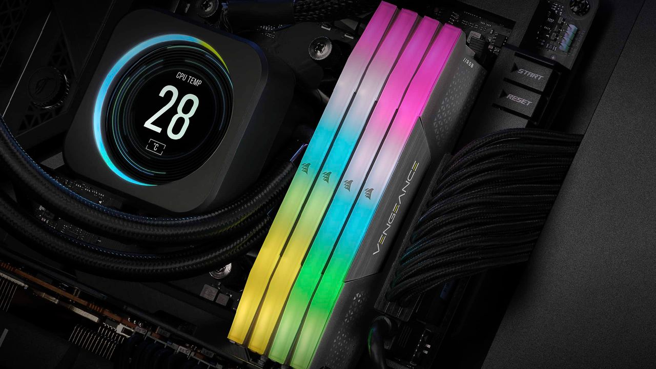
When it comes to building a new PC, memory has seen the sharpest rise in pricing in years. Now, you have to seriously consider the cost of the RAM kit in your build, and especially for those stepping up from a DDR4 platform, whether the cost is worth it for the extra performance. Currently, the prices continue to rise with no end in sight. It's hard to suggest holding off on upgrading now, as we have no clue when the prices will start to fall - if at all. However, if you are looking for a brand new pair of DDR5-6000 RAM sticks for a desktop PC, then Corsair's Vengeance 32GB DDR5-6000 kit has just received a $215 discount that brings the price down to $401.99, from its $616.99 list price. This makes it the cheapest 32GB DDR5-6000 kit that you can purchase today.
The kit includes two 16GB DDR5 modules that run at 6000 MT/s with a CAS latency of CL36 and further timings of 38-38-76. Corsair's Vengeance kits are a popular choice among PC building enthusiasts and feature black aluminum patterned heat spreaders with RGB lighting running across the spine of the sticks. They come with Intel XMP BIOS profiles for preconfigured overclocking.
Corsair's Vengeance memory kit consists of two 16GB sticks for a total of 32GB. The kit has a CAS latency of CL36 and further timings of 38-38-76, with a voltage of 1.25V. View Deal
Prices of memory, especially DDR5 kits, are very off-putting at the moment, and looking at upgrading can feel the same. With current-gen game consoles going up in price, expectations for next-gen consoles are that the prices will stretch over a thousand dollars. So if you're thinking of getting a new gaming PC or upgrading from an older DDR4-based system, it's probably best not to wait around. Just be prepared for some hurt to the bank account. Industry figures say the memory shortage could last for years or even a decade, with no relief at all in sight; prices are much likelier to go up rather than down.
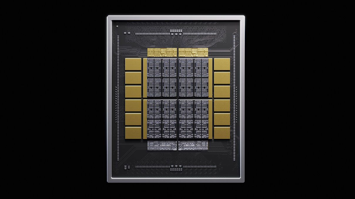
Nvidia's NVLink Fusion program gives the company's partners the building blocks necessary to connect custom chips with the NVLink scale-up domain used to join many separate processors into a single coherent system like the Vera Rubin NVL72 rack-scale accelerator. Today, Nvidia is adding a new building block to that toolkit: NVHBM, a custom implementation of the high-bandwidth memory that underpins practically every AI accelerator in use today.
As Nvidia describes it, NVHBM is a custom HBM base die that promises higher bandwidth, lower power usage, and a smaller on-die footprint than traditional HBM4e. Nvidia says it's designed and validated with "leading memory vendors," so it promises custom silicon developers faster time-to-market than implementing commodity HBM from the ground up. But it's worth re-emphasizing that this isn't an HBM replacement. Instead, it's a new building block that Nvidia is only offering to its custom silicon partners.
Memory bandwidth is everything for AI accelerators, and NVHBM promises up to 30% higher bandwidth per stack than standard HBM4e. For memory-bandwidth-bound AI workloads, that higher bandwidth translates into higher throughput, such as a higher tokens-per-second rate for AI inference.
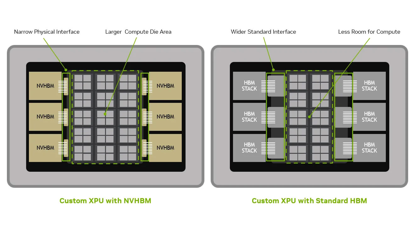
The custom NVHBM base die also reduces the footprint of memory-related circuitry on the main custom accelerator die. Traditionally, the HBM memory controller has been incorporated into the primary silicon die on the package. NVHBM instead moves the memory controller into the base die of the HBM stack and provides a smaller custom PHY that NVLink Fusion customers can then integrate into their designs.
(Image credit: Nvidia)
Nvidia says this approach frees up precious package real estate that can then be used for additional compute die area — up to 30% more compute on the primary silicon die. NVHBM further promises to simplify the interposer routing used to join multiple chips together for designs using advanced packaging techniques.
NVHBM also provides power savings versus off-the-shelf HBM4e stacks. As Nvidia has continuously hammered home in the Vera Rubin roll-out, every watt that isn't going into token production is a watt wasted. Nvidia says NVHBM uses 15% less power than commodity HBM4e, and that power savings can be banked for performance-per-watt improvements, reallocated into more functional units for a custom accelerator design, or translated into higher sustained performance within the same power budget.
Higher bandwidth at lower power is a huge win for AI accelerators that are moving massive data structures like model weights and KV caches around, especially when those savings are multiplied across many thousands of chips. The energy saved on data movement can be plowed back into higher performance from the accelerator itself or reallocated to support larger numbers of accelerators within the same fixed power envelope.
But these are, as of now, reasons for Nvidia's prospective partners to consider incorporating NVLink Fusion and NVHBM into their custom designs, not benefits that will materialize in the Rubin rack-scale systems already in production.
Along with NVHBM itself, Nvidia announced that Amazon's Annapurna Labs will be its first partner on NVHBM. , and Annapurna VP Nafea Bshara says: “We look forward to this technology collaboration to benefit future AWS infrastructure designs.” Annapurna's next-generation Trainium 4 AI chips will already support the NVLink Fusion scale-up interface, so it seems likely that follow-on chips will support NVHBM, too.
Earlier this month, Samsung introduced the industry's first LPDDR5X-PIM memory, adding in-memory logic to the low-power memory standard, and at Hot Chips 2026, it dove into the memory technology that we've previously seen at play through HBM stacks.
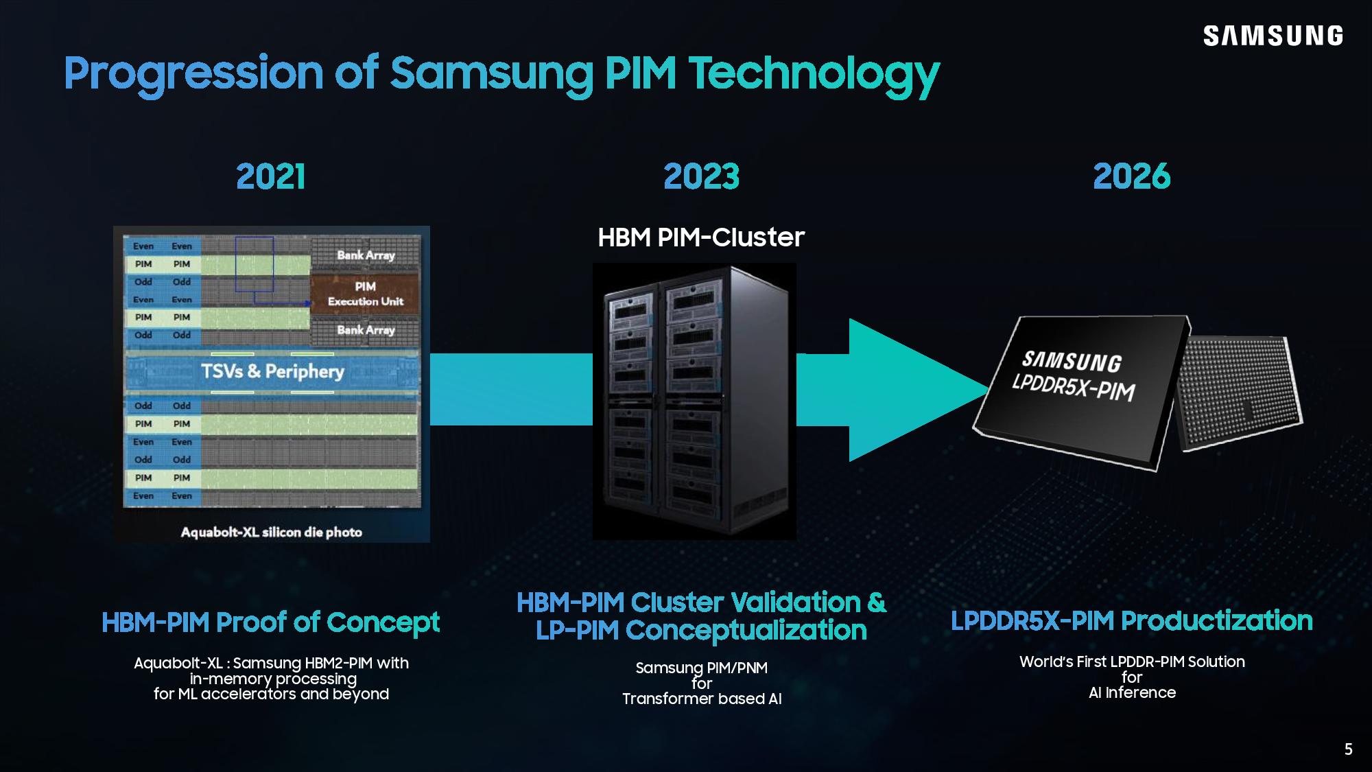
PIM, or Processing-in-Memory, is a technology Samsung demoed as early as 2021, piloted through HBM stacks in AMD accelerators. It's a small bit of logic that sits alongside DRAM cells, allowing basic calculations to happen directly in-memory. By handling those basic calculations locally, Samsung is able to eliminate the processor as a bottleneck and speed up, in particular, AI inference. In inference tasks, Samsung says its LPDDR5X-PIM is 2.28x faster than standard LPDDR5X, in fact.
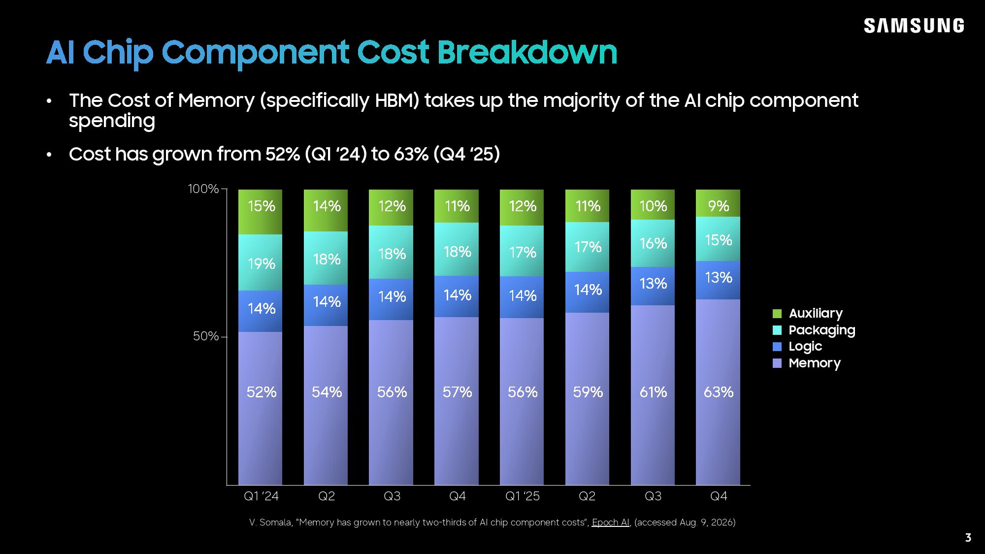
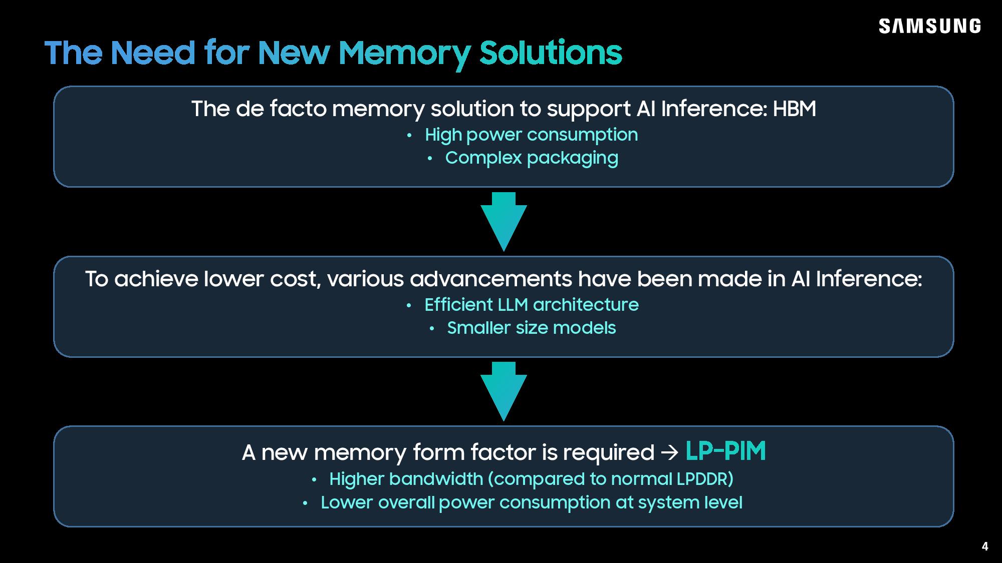
The reason for adding in-memory processing to LPDDR5X is pretty clear: HBM is too damn expensive. Micron warned just a day earning at Hot Chips that the HBM wafer demand is only getting worse, and Samsung opened its presentation with something we're all well aware of. Memory makes up the bulk of AI chip costs, and its share of the pie continues to grow. Add on top of that the power demands of DDR5, much less HBM, and LPDDR5X seems like an ideal target for PIM.
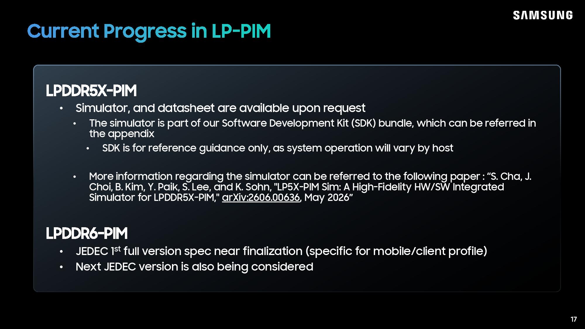
Samsung introduced HBM-PIM in 2023, and at the time, introduced the concept of LPDDR5X-PIM. What it shared at Hot Chips is a real product, taking the concept of LPDDR5X-PIM and putting it through validation. Samsung is also looking ahead for LPDDR6X-PIM, and the company says it hopes to have an initial specification from JEDEC this year.
Bringing in-memory processing to Samsung LPDDR5X
(Image credit: Samsung)
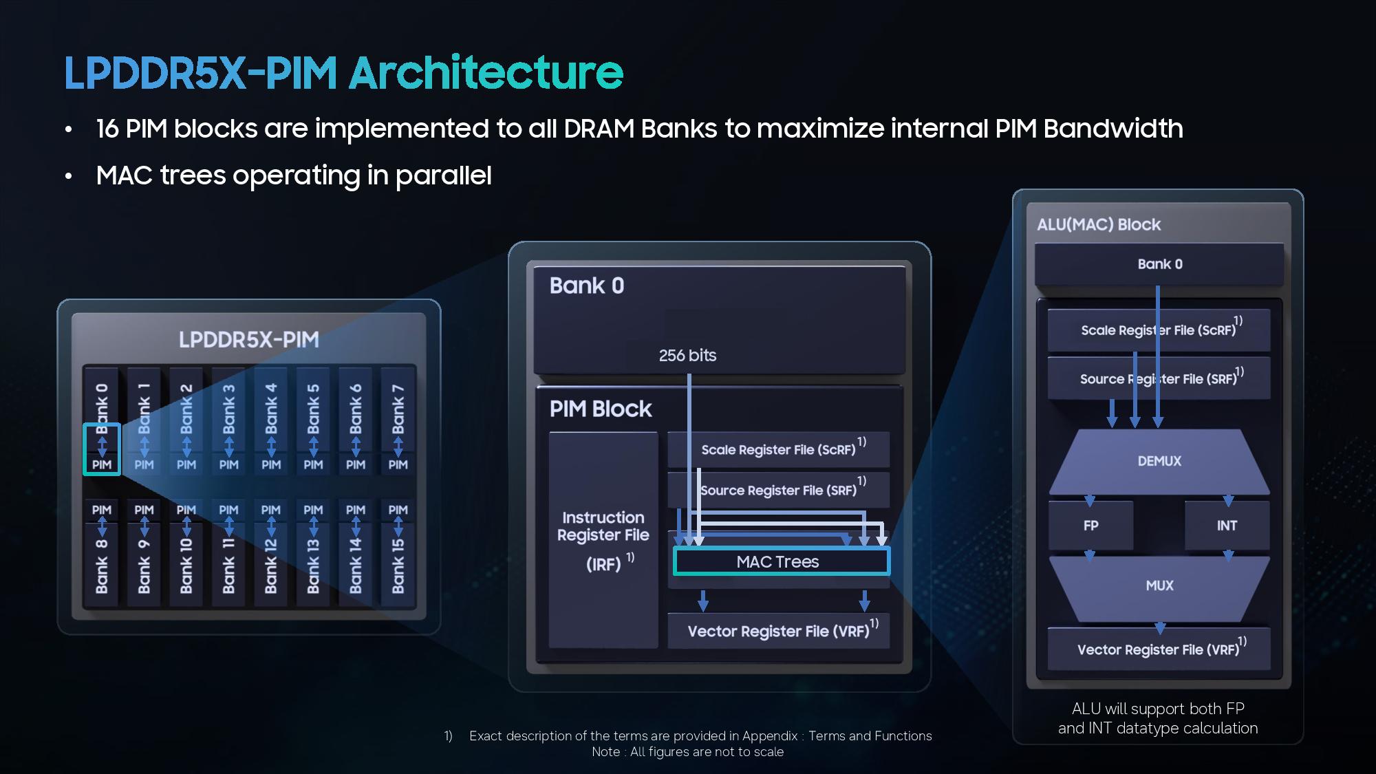
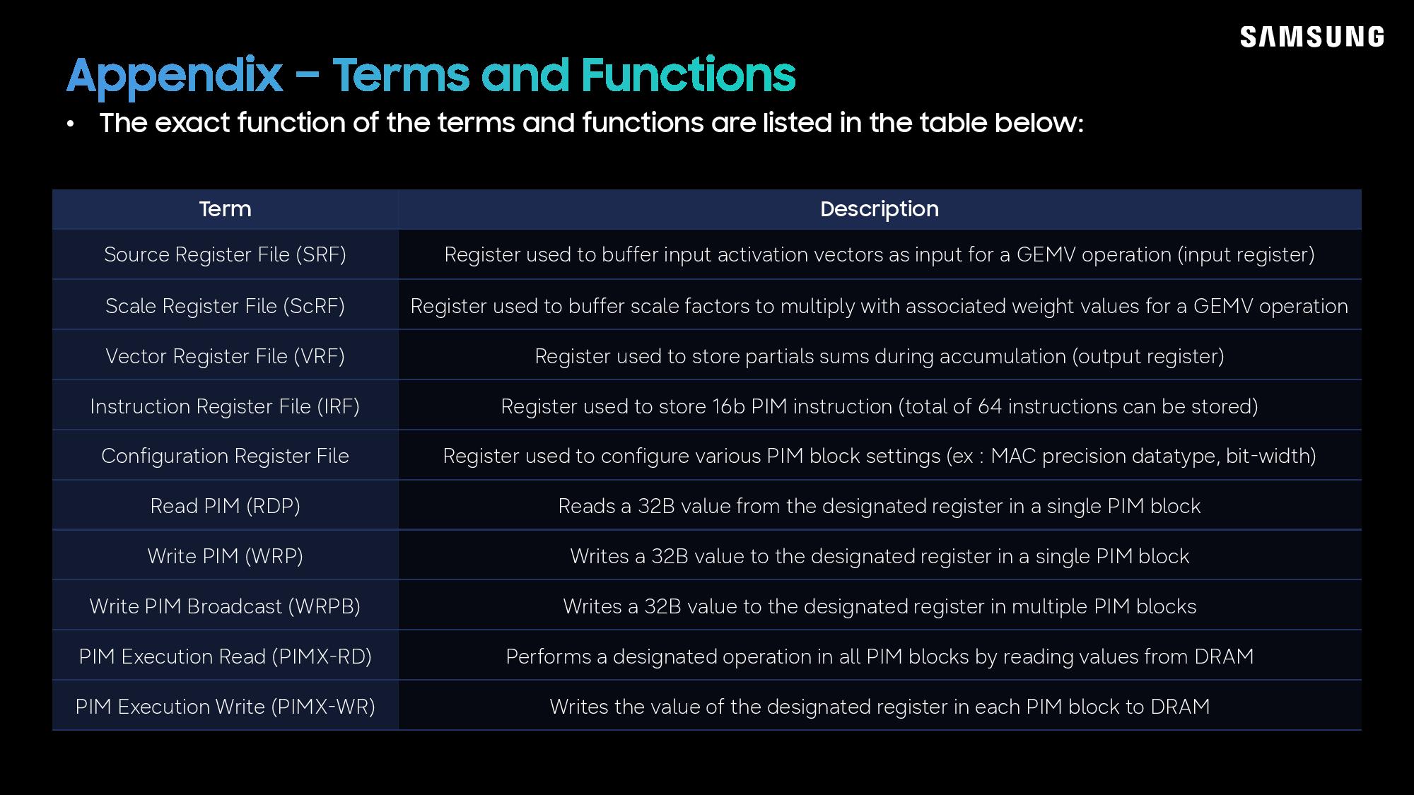
Above, you can see a basic layout of how Samsung integrated PIM into LPDDR5X. Each memory bank has its own PIM, which is an advancement over HBM-PIM, where Samsung had to cut banks to fit the logic. The memory bank, scale register file, and source register file feed parallel MAC trees. Once calculated, the output (either integer or floating point output) is written to a vector register file.
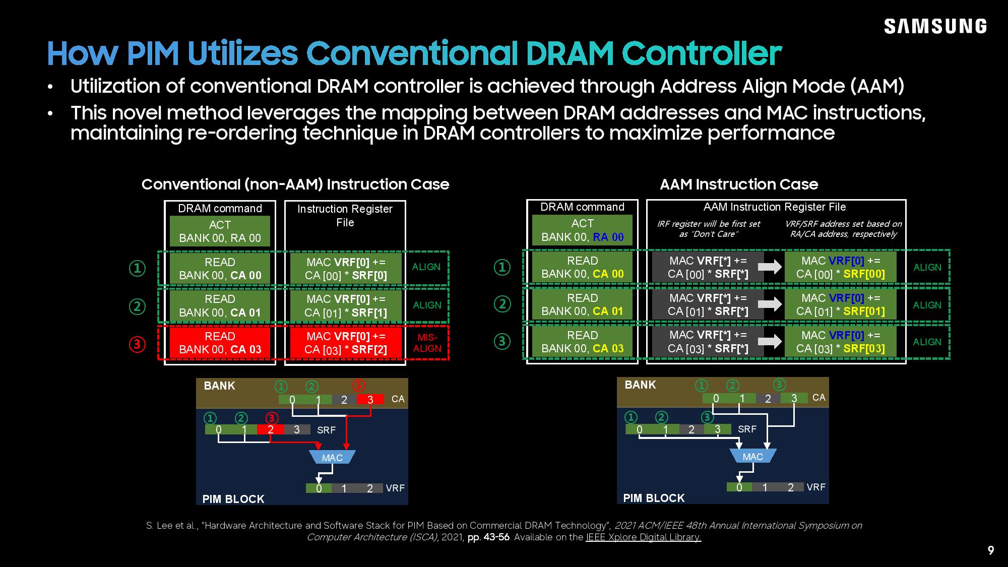
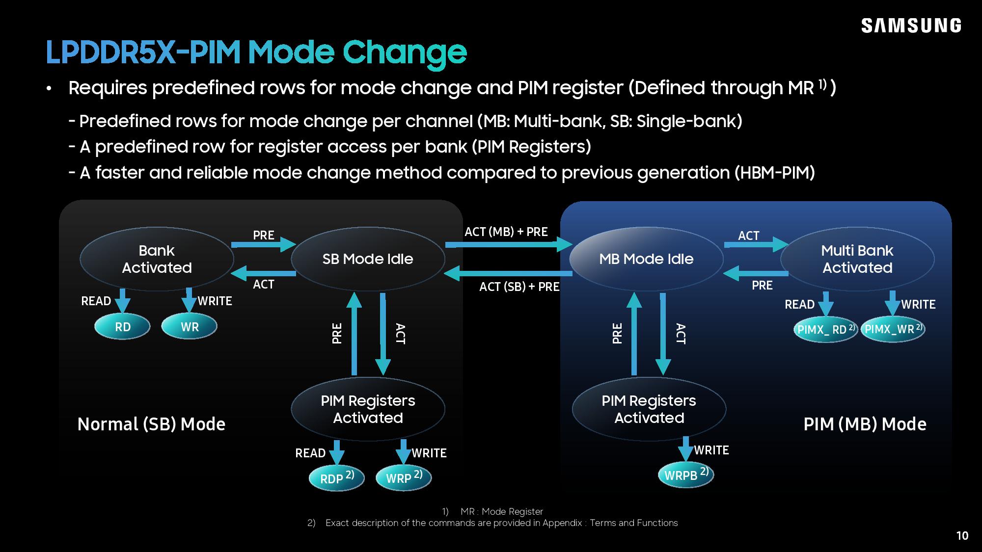
Samsung says its LPDDR5X can operate in two modes: single-bank (traditional DRAM) or multi-bank (PIM). Traditional DRAM controllers work, with commands switching between standard read/write or a PIM read/write depending on the mode. The challenge, according to Samsung, was reordering with conventional DRAM.
Samsung uses what it calls Address Align Mode (AAM) to get around the reordering issue. It maps DRAM addresses to MAC instructions, assigning the VRF/SRF address based on the RA/CA address, respectively, and not the Instruction Register File.
(Image credit: Samsung)
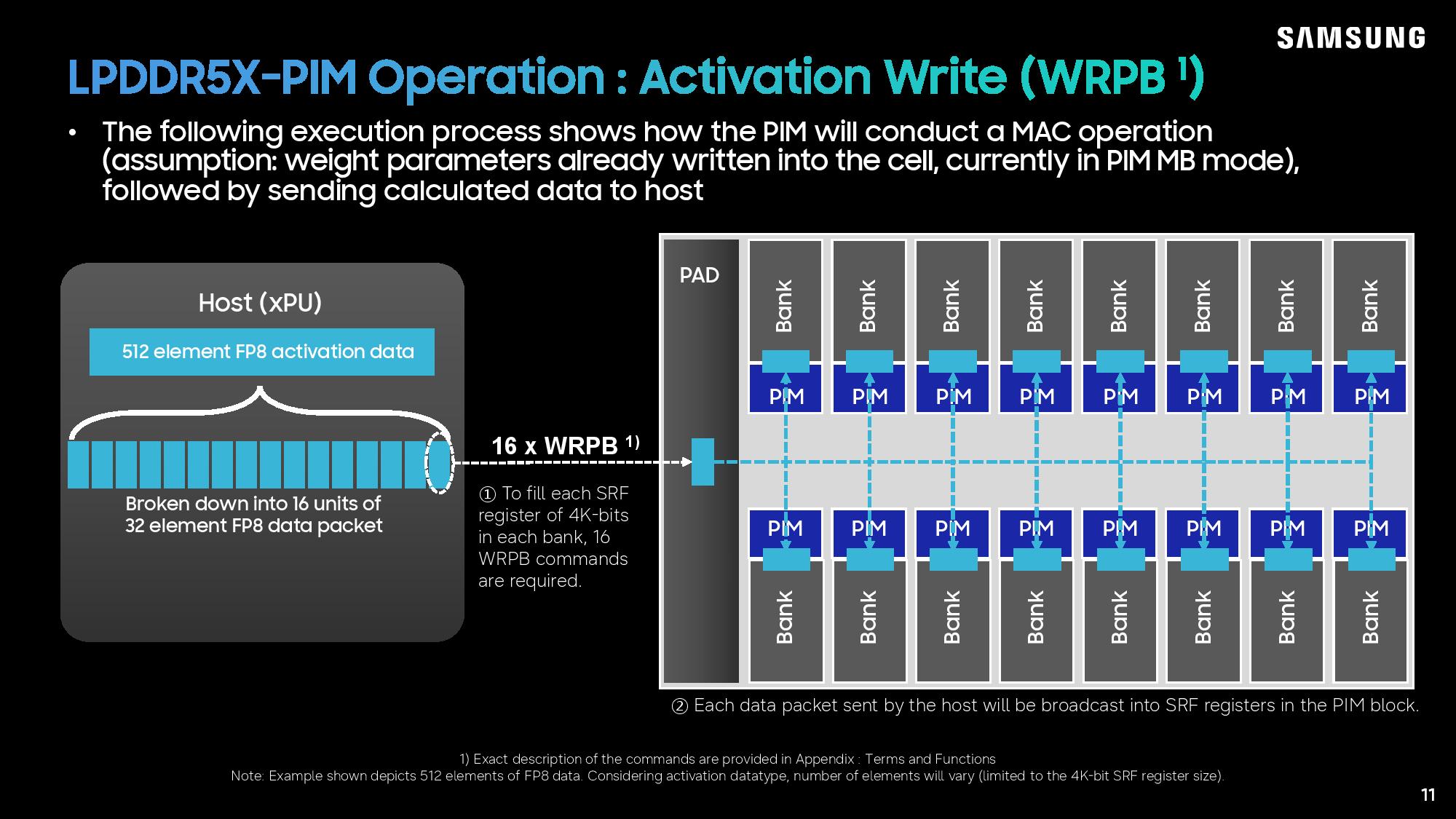
To demonstrate how data moves through the memory cells and calculations are performed, Samsung provided an example of a MAC operation, assuming weight parameters for the data are already written into the cell, and the memory is operating in multi-bank (PIM) mode.
(Image credit: Samsung)
Storing 512 bytes of FP8 activation data, it's first broken down into 16, 256-bit packets, which are written into each of the banks in and noted in the Source Register File.
(Image credit: Samsung)
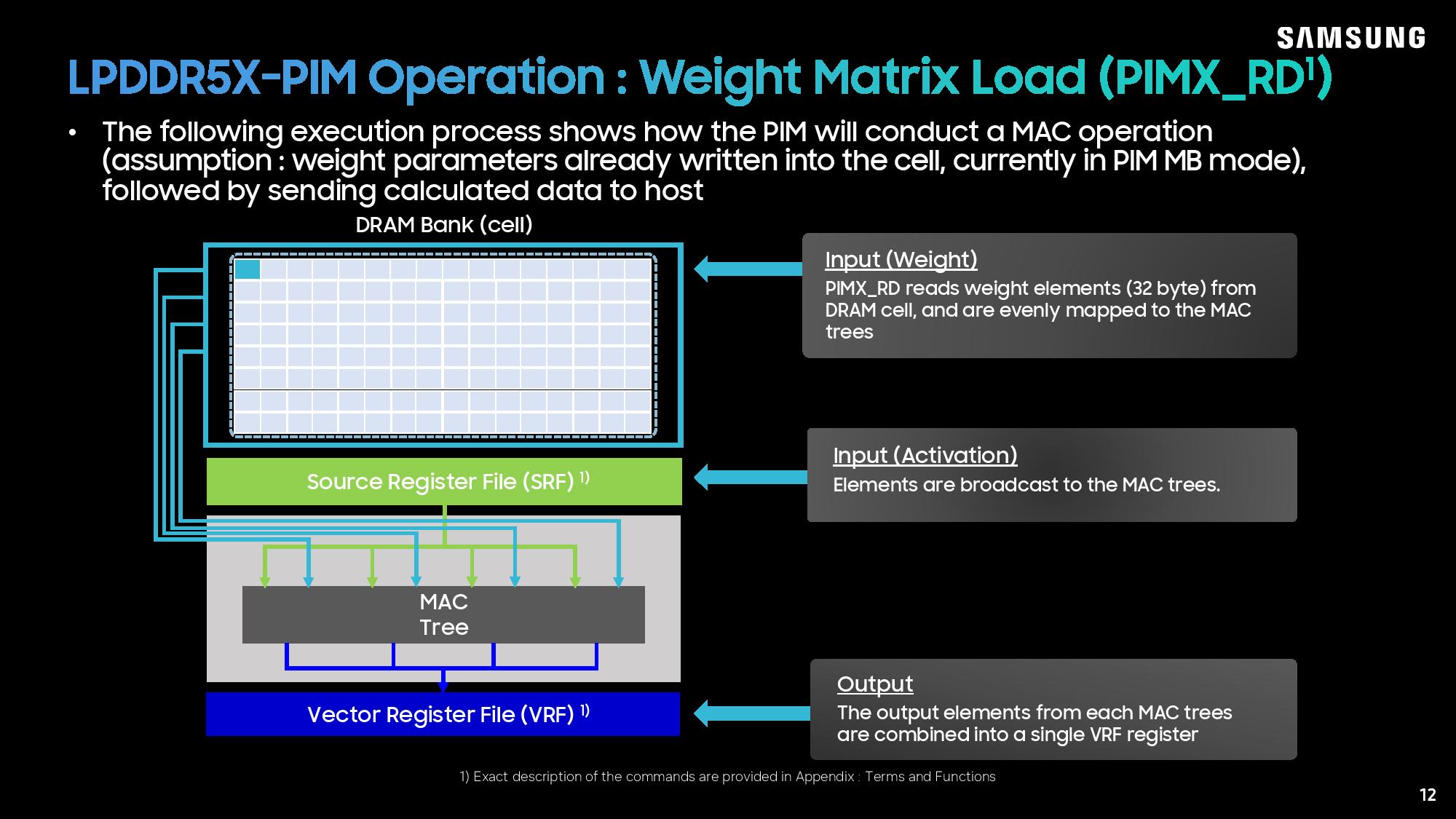
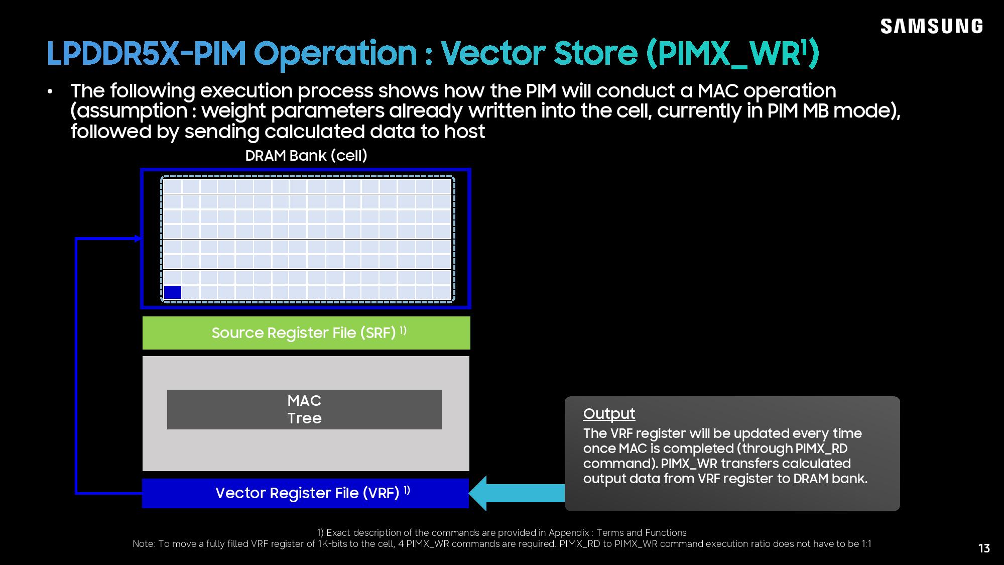
A PIMX_RD reads the weight data from the DRAM bank, feeding into the MAC trees alongside the data from the SRF. Once the calculation is done, the output vector from each operation is written into the Vector Register File.
(Image credit: Samsung)
Once the calculation is done, a PIMX_WR command transfers the output data back to the DRAM bank. Samsung noted there doesn't need to be a 1:1 relationship between reads and writes, but it's useful for this example. With a VRF size of 1 kbit, a maximum of four calculations can be written to the VRF.
(Image credit: Samsung)
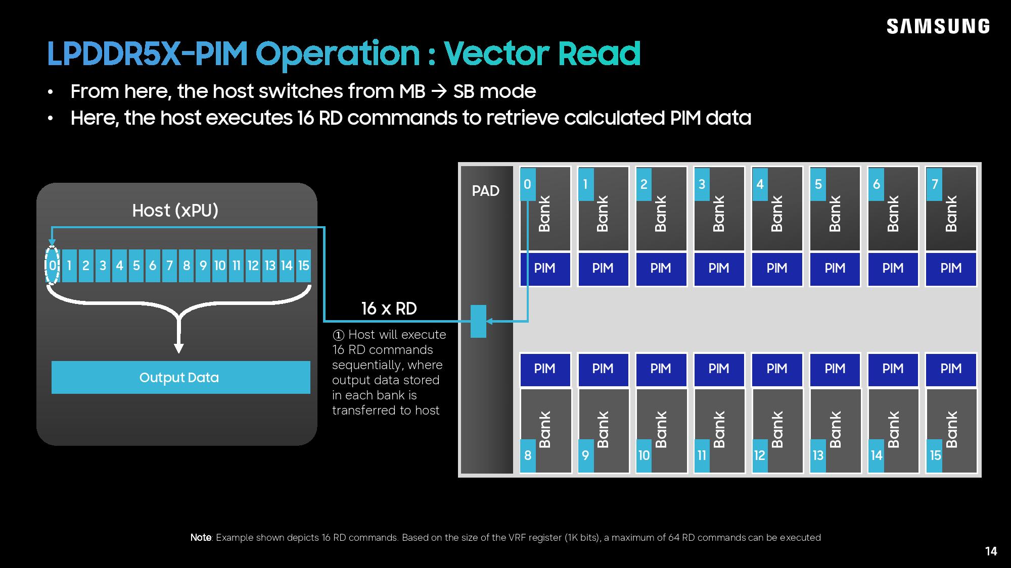
With the output written back to memory banks, the host just needs to read the data from memory. The host switches to single-bank (conventional DRAM) mode and executes 16 reads to gather the output from all of the memory banks.
Samsung LPDDR5X specs and preliminary performance
(Image credit: Samsung)
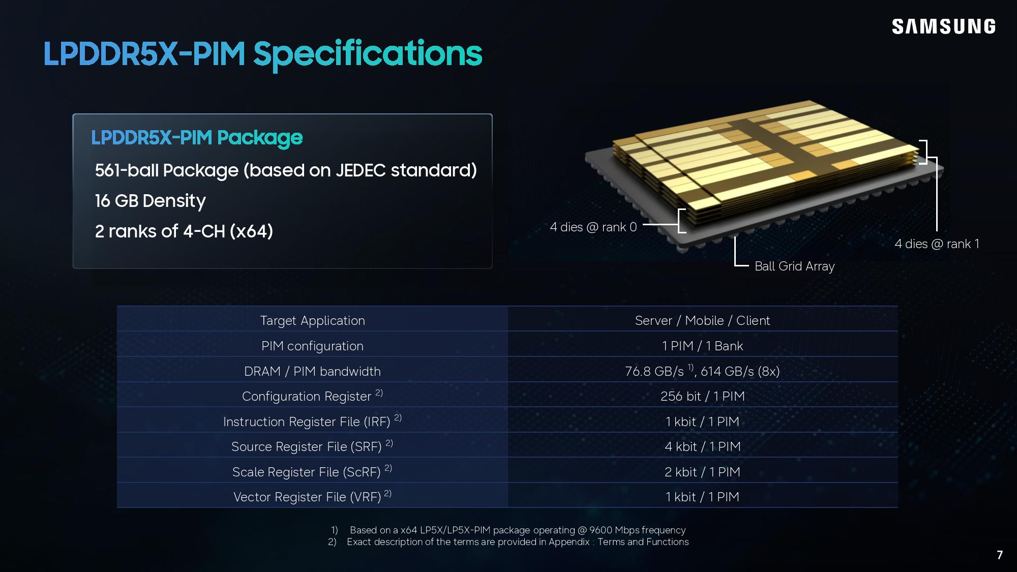
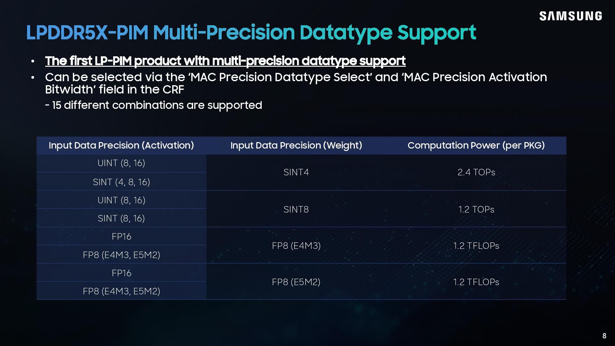
Samsung's LPDDR5X-PIM looks a lot like LPDDR5X. It uses a standard 561-ball array for packaging, just like LPDDR5X, and Samsung uses two 64-bit ranks with 16 GB modules. The critical number here is bandwidth. With LPDDR5X-9600, peak bandwidth is 76.8 GB/s, but that's increased by eightfold with PIM to 614 GB/s by reducing data movement and keeping basic logic local.
Samsung uses four dies per rank, for a total of eight dies. Not the various registers above, as well, as they're important for the illustration of data flow through Samsung's LPDDR5X-PIM memory.
(Image credit: Samsung)
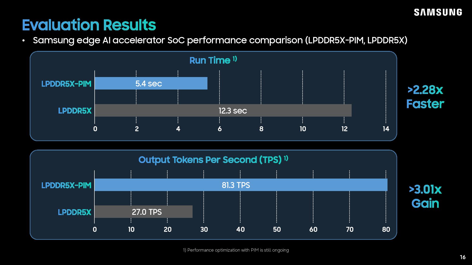
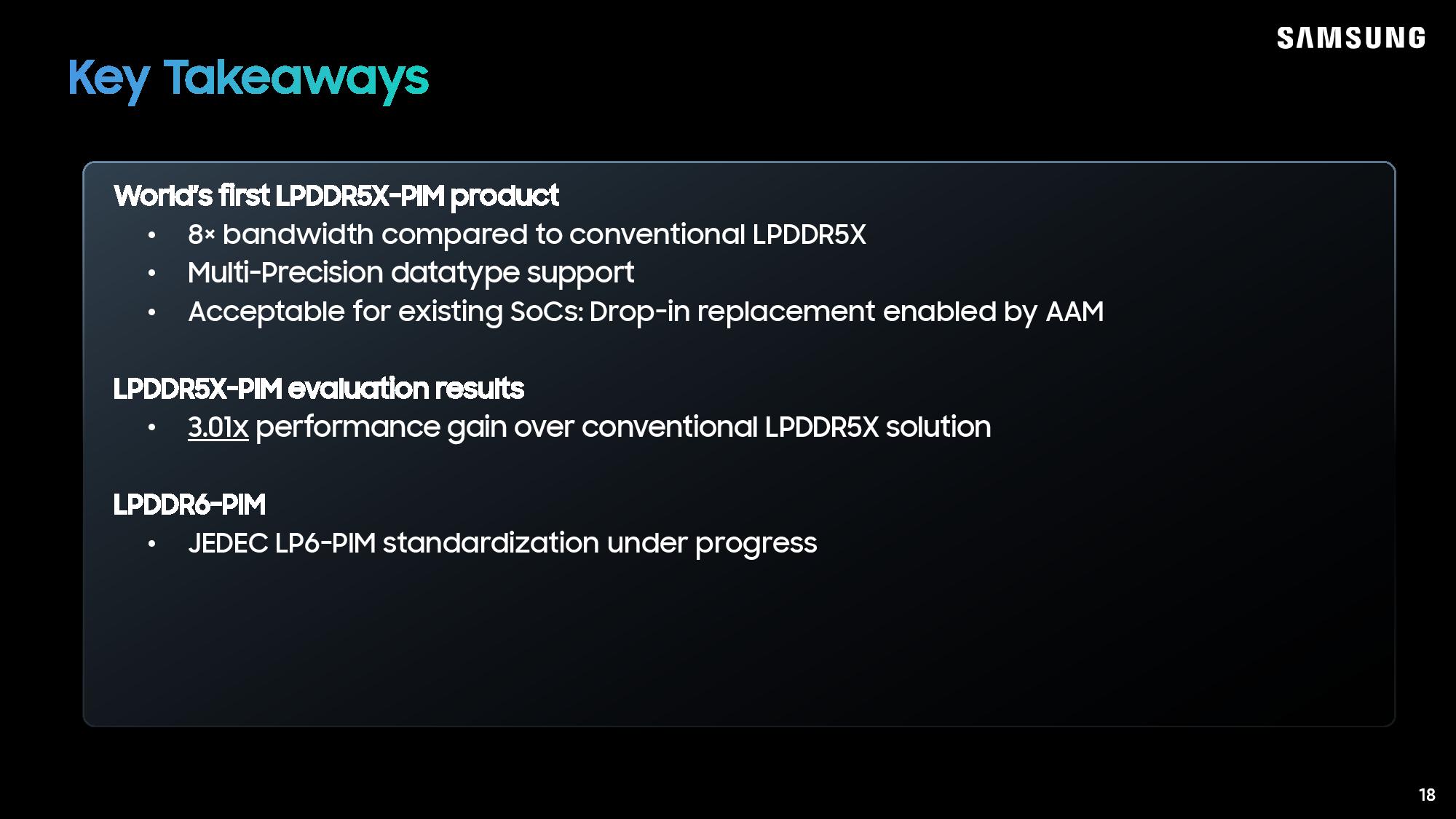
In Samsung's preliminary benchmarks, LPDDR5X-PIM is impressive. In model run time, Samsung say a 2.28x improvement with PIM, and in tokens per second (TPS), PIM offered a 3.01x increase in performance.
(Image credit: Samsung)
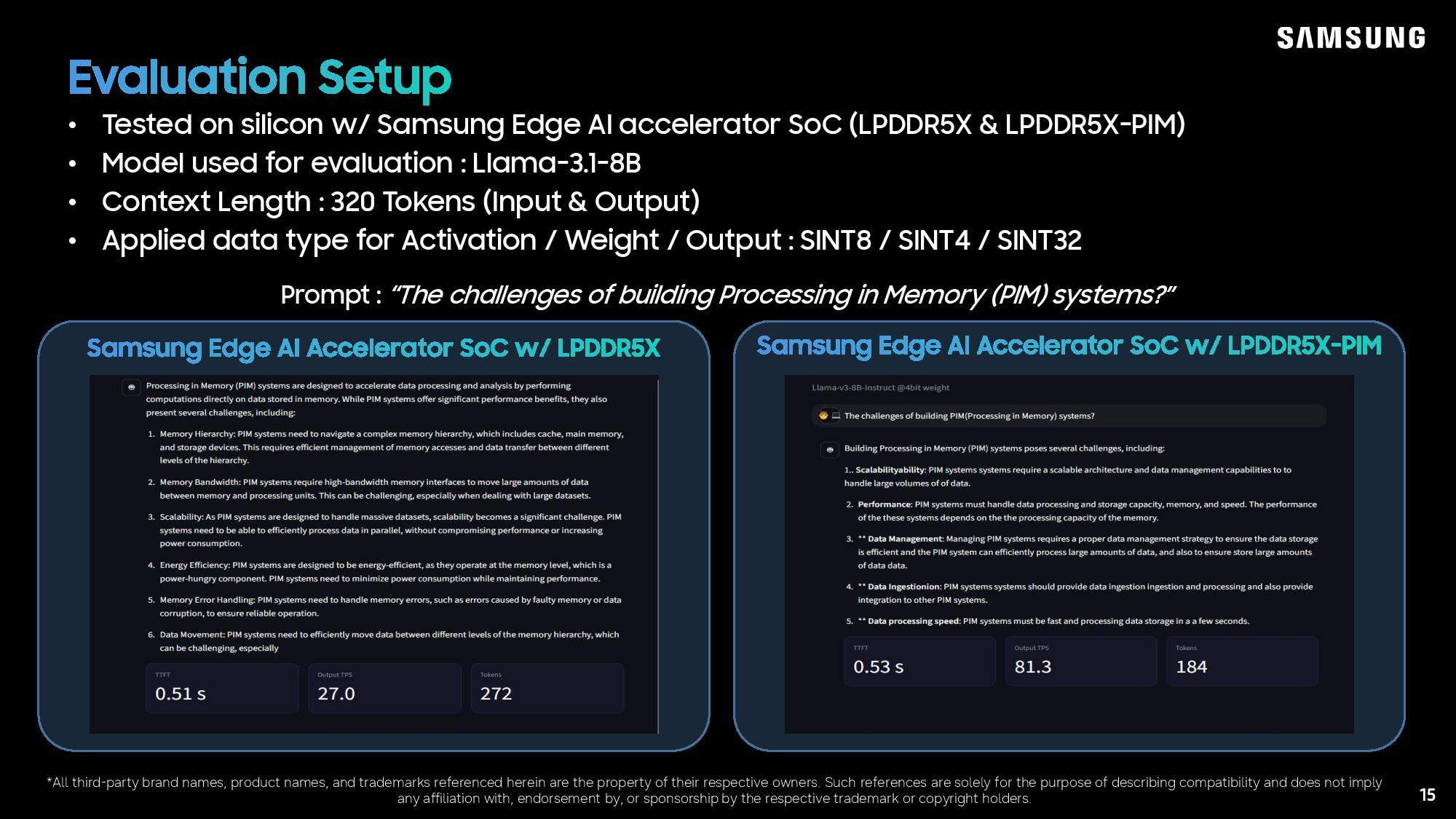
The slide above shows what happened behind the scenes to gather these numbers, with Samsung using an edge AI accelerator — we're not sure which, but perhaps an early Gaia SoC — and testing Llama 3.1 with 8 billion parameters. Notably, the output is different, which one attendee pressed Samsung about. The company says optimizations are ongoing to improve accuracy, but it expects the performance benefit to remain the same.
One of the main advantages of LPDDR5X is right there in the name: low power. With PIM, power consumption becomes more of a concern, but Samsung says it doesn't expect higher power consumption overall compared to conventional DRAM. The presenter noted that peak power consumption will be "much higher" due to the bursty power draw of the PIM, but Samsung still expects overall power draw to be lower than conventional DRAM.
That comes down to extra reads/writes. Although PIM represents a power increase, decreasing the number of times data needs to move between DRAM and the host will lead to overall lower power consumption. "We're not having significant power increase," as Samsung's Karam Hwang put it.
LPDDR5X has, until recently, only had applications in consumer products. However, SOCAMM2 serviceable modules allowed Nvidia to use LPDDR5X as the memory of choice with its Vera CPU. And Intel uses LPDDR5X with its new Crescent Island AI accelerator.
Even with PIM, LPDDR5X doesn't come remotely close to the bandwidth with available with HBM, but it has a lot of applications elsewhere. Samsung's targets of server, client, and mobile are telling, with LPDDR5X-PIM accelerating edge AI on mobile and client devices, as well as arriving in lower-scope accelerators like Crescent Island.
When it comes to building a gaming PC, DDR5 RAM clocked at speeds of 6,000 MT/s is often touted as the sweet spot for specs. While slower and faster speeds are available, it's very much the benchmark for both price and performance, which is why it's noteworthy that this particular configuration now costs $400, a more than 400% increase from the low prices we've seen in the past.
In addition to our ongoing RAM price tracking, we perform daily spot checks on pricing for discounts or deals for 32GB (2x16GB) of DDR5 RAM, given its aforementioned significance as the "benchmark" when it comes to capacity. In recent weeks, the price of 32GB DDR5 6000 RAM has been creeping ever closer to that unfortunate $400 milestone, and in the last few hours we've just crossed the threshold. That's not to say that prices might fluctuate back down in a day or two, but generally the traffic is only moving in one direction.
You can buy 32GB of DDR5 RAM at slower speeds for less — this Corsair Vengeance DDR5 4800 is"just" $359 — but good RAM is now harder (and more expensive) to come by than ever before.
According to data from PCPartPicker, this particular 32GB DDR5 6000 kit from Corsair has been as little as $80 in years gone by at Newegg, marking a full 400% price increase on the lowest we've ever seen on this model.
All signs point to the memory shortage, and thereby pricing, getting worse in the coming months. As such, bundles and pre-built PCs remain one of the only ways to insulate yourself from cost increases if you're in the market for new hardware. As mentioned, slower memory speeds are available at lower prices, but compromising for 4,800 MT/s RAM to save $40 when building a PC is an extremely tough state of affairs.
Only one piece of it is new: the Bravera SC6 PCIe 6.0 SSD controller, which samples in Q4. Structera X has been shipping since 2024, the Structera S switch was announced at OFC in March, and the Photonic Fabric optical memory tier came with the Celestial AI acquisition in February. Meta, the reference customer for the use case Marvell is selling, did it with an ASIC of its own design rather than anything from Marvell.
What's new (and what isn't)
The Bravera SC6 is a PCIe 6.0 x4 controller with 16 NAND channels, eight chip enables per channel, a 3,600 MT/s ONFI and Toggle interface, and 12 Arm Cortex-R82 cores plus three Cortex-M7s, according to Marvell's product blog.
Marvell says it doubles the Bravera SC5, supports NAND from multiple suppliers, and uses a host-managed flash translation layer, meaning cloud operators control write placement, garbage collection, and wear leveling themselves, with KV cache spillover from HBM to SSD as the primary workload. Sampling starts in Q4 2026, which puts drives in 2027 at the earliest on the timeline Tom's Hardware Premium laid out for the PCIe 6.0 controller field, where Phison and Silicon Motion are chasing the same Gen6 drive launches.
Structera X 2404 and X 2504, the DDR4 and DDR5 expansion controllers, were announced in July 2024, and Marvell's FMS blog says both are in hyperscaler deployments, with inline LZ4 compression that Malik told EE Times yields roughly 2 to 2.5 times the effective capacity.
The Structera S 30260 switch, announced at OFC in March, carries 260 PCIe 6.0 and CXL 3.x lanes, connects 16 or 32 CPUs or GPUs to up to 48TB of shared memory at 4 TB/s aggregate bandwidth and under 460ns round trip, and begins sampling this quarter. Photonic Fabric came in with the $3.25 billion Celestial AI acquisition that closed in February, with Marvell now describing it as a shared-memory tier reaching up to 50 meters with up to 32 TB of warm KV cache and a claimed 2 to 3 times token throughput inside existing footprints. Marvell also took a $2 billion investment from Nvidia in March, tied to NVLink Fusion, the proprietary scale-up fabric CXL pooling has to sit alongside.
DRAM contract prices have tripled since Structera launched
Conventional DRAM contract prices rose 90% to 95% quarter-on-quarter in Q1 2026, the steepest increase on record for every DRAM category. Q2 added another 58% to 63%, and server DRAM is set to climb a further 13% to 18% in Q3, held in check mainly by the long-term agreements U.S. hyperscalers signed to cap pricing through 2027 and 2028. Server DRAM buyers in the U.S. and China were receiving about 70% of their orders late last year as suppliers diverted wafers to HBM.
Samsung, SK hynix, and Micron have all been winding down DDR4 output since last year, and TrendForce put the legacy memory rally at up to 50% for DDR4 in Q1 alone. A module pulled from a decommissioned 2021 server is now worth a multiple of what it was when Structera X was announced, and the DDR5 that would replace it has roughly doubled in price twice. When Marvell first pitched DDR4 reuse in 2024, it was a sustainability line item, but two years later, the memory crunch has turned it into a capex line item.
Meta's recycling numbers
Meta's Vistara ASIC, presented at ISCA 2026 in late June, is a CXL 2.0 Type-3 expander on a PCIe 5.0 x16 link that bridges two DDR4 channels to a host and runs at 128GB per chip using 32GB modules recovered from retired machines. Each MemServer pairs a 158-core AMD EPYC Turin with 768GB of local DDR5-6400 and 256GB of CXL-attached DDR4-2400, and Meta claims idle round-trip latency of around 50ns on the controller path.
The paper states that around 40% of Meta's fleet is memory-capacity bound, that its servers last three to five years while the DRAM inside them is good for seven to 10, and that the deployment cuts server counts by up to 25% for disaggregated ML inference, average latency by 29% for distributed caching, and job failures by 33%, The Register from the paper ahead of the talk.
Malik told EE Times, "The first and foremost important use case within CXL is the recycling of DDR4," and Marvell's FMS release says Structera X was "developed in close collaboration with leading hyperscalers" without naming one. Meta's paper describes an in-house ASIC, an in-house MemServer chassis, and an in-house Linux page-placement stack, the full path one would take when volume justifies its own silicon, while Astera Labs' Leo controllers reached Microsoft Azure's M-series preview in November last year.
CXL's deployment gap
SemiAnalysis declared CXL dead for AI in March 2024 because Ethernet-style SerDes such as NVLink carry roughly three times the bandwidth per millimeter of die edge as PCIe 5.0 or 6.0, so every CXL lane on an accelerator costs scale-up bandwidth that could have gone to the GPU-to-GPU fabric instead.
Marvell's CXL pitch accordingly targets CPU-side capacity and KV cache staging rather than the GPU-to-GPU path where you’ll find NVLink Fusion. Yole estimated two-thirds of servers sold in Q1 2025 were CXL-capable and expects more than 90% to be by the end of this year, yet it puts the share of servers actually using CXL at close to zero today and only 13% by 2030.
Marvell's benchmarks for the Structera S show a 16TB pooled DRAM tier delivering 4.8 times the inference throughput and an 82.7% cut in time to first token in GPU configurations, attributed to keeping KV cache in DRAM instead of recomputing or reloading it. Those are vendor numbers with no disclosed model or baseline, and the switch only starts sampling this quarter. Nvidia, AMD, and the SSD makers all offer their own routes for the same cache spillover.
Nvidia has told some of its largest customers that the prices of servers containing its AI chips will rise by more than 15% in many cases,Bloomberg reported on Saturday. The increases will take effect on Grace Blackwell and Vera Rubin systems shipping early next year, according to people familiar with the matter, who commented on communications that have not yet been made public. The size of each increase will depend on the chip generation and the memory configuration involved. Companies that build servers under contract for large data center operators, including Microsoft, Google, and Oracle, have recently notified their customers of the forthcoming increases, the people told Bloomberg.
This is another example of the so-called "RAMageddon" that's gripping the DRAM market, with contract prices having risen at record rates this year. Analysts projected that conventional DRAM contract prices would climb 58% to 63% quarter-over-quarter in Q2 2026, following a Q1 surge of 90% to 95%, as suppliers reallocated capacity toward HBM and server products. SK hynix said in October last year that it had already sold out its entire 2026 memory production capacity, and Samsung and SK hynix raised 2026 HBM3E supply prices by close to 20% before the year began.
(Image credit: Tom's Hardware)
AI systems carry enormous memory loadouts, with Nvidia's Rubin GPU shipping with up to 288GB of HBM4 per package, and the NVL72 rack-scale system combines 72 of those GPUs, putting more than 20TB of HBM in a single rack before accounting for the LPDDR attached to its Vera CPUs. With HBM production consuming roughly four times the wafer area of equivalent conventional DRAM, memory has become one of the largest line items in an AI server's bill of materials, and it's continuing to rise at a stratospheric pace.
Ironically, the supply crunch that's now inflating Nvidia's systems is the same one its demand helped to create. The three major memory makers spent this and last year shifting advanced nodes and new capacity toward HBM and high-capacity server DRAM, starving commodity markets in the process. Consumer DDR5 pricing has more than doubled since late 2025 as a result, with a mainstream 32GB DDR5-6000 kit selling for around $392 in August against $110 to $140 a year earlier, according to our RAM price tracker.
Nvidia has already passed rising costs through to consumers, raising prices on GeForce graphics cards earlier this month. The Bloomberg report indicates the same unrelenting pressure has now reached the top of the Nvidia stack, where hyperscalers as well as PC builders will be absorbing the increase. A 15% rise on rack-scale systems that sell for several million dollars each adds hundreds of thousands of dollars per rack across deployments that run to thousands of racks.
Nvidia runs a gross margin of roughly 75% non-GAAP, among the highest in the semiconductor industry, and the reported hikes indicate the company intends to pass memory cost inflation on to customers rather than absorb it, which it can more than afford to do. Meanwhile, supply of its accelerators from TSMC still can't meet demand, which limits buyers' immediate leverage.
Whether the increases push hyperscalers further toward AMD's accelerators or their own custom silicon will depend on how quickly those alternatives can absorb displaced demand, and all of them draw HBM from the same three constrained suppliers.
 登录
登录