Some 700 Micron employees in Taiwan will receive five years’ worth of salary in bonuses as the company announced three bonuses in a single payout. According to Digitimes, this accounts for about 17% of the over 4,300 production-line employees working at Micron Taiwan. The remaining staff will not come out empty-handed, though, as they will receive three bonuses in the month of October. The news comes as Micron continues to battle worker unrest and unions fighting for increased pay.
The lump-sum payout consists of three incentives — an annual performance bonus that’s estimated to be between 7.5 and 12.5 months of salary for the majority of workers, a mass-production bonus amounting to 20% of their annual salary, plus a one-time $31,000 (NT$1,000,000) appreciation bonus which will be prorated for employees who haven’t reached a full year of service. Micron workers across the globe also expect a new quarterly profit bonus which will be paid 50% in cash and 50% in stock. This bonus will start in January 2027, with the first one to be paid 100% in cash.
Micron is following in the footsteps of Samsung and SK hynix, which have recently paid out massive bonuses to their workers of up to $400,000. This is a direct effect of the AI-driven memory chip boom, which saw the big three memory chip manufacturers — Micron, Samsung, and SK hynix — raking in massive orders from AI hyperscalers. The record profits that these companies are drawing from the appetite for AI data centers have led workers on production lines to demand a slice of the pie. Samsung workers voted to accept a $340,000 average bonus in May 2026, while SK hynix workers are set to receive $477,000 in bonuses this year, which could potentially grow to almost $900,000 in 2027.
Despite this seemingly massive payout, the workers’ union at Micron Taoyuan is still in the midst of a dispute with management regarding their pay. Some officials of the group have already launched a one-day strike as they call for clearer profit-sharing arrangements and terms for bonuses, with nearly 70% of members at the Taoyuan site turning down management’s latest offer. The two sides are tentatively set to meet on November 6 again for further negotiations. On the other hand, the union at Micron Taichung has already agreed to a 10% employer’s contribution towards worker pensions and a tripling of their day-shift allowance.
These bonuses allow workers to get a share of the massive profits that the chipmakers are raking in at the moment, allowing them to stay competitive for chip talent. However, their reliance on performance and profit bonuses also means that these incentives could fall precipitously if AI demand falls and the demand cycle returns to normal.
TSMC is weighing raising prices for its Chip on Wafer on Substrate (CoWoS) advanced packaging technology by as much as 20%, reports Trendforce, citing supply chain sources and local media. The increase reflects strained capacity amid AI demand and longer delivery times for chipmaking tools. Such a hike would be significant, as CoWoS is already one of the tightest links in the AI supply chain. TSMC has yet to confirm the report.
CoWoS combines logic dies and high-bandwidth memory (HBM) stacks within a single package, which is how AI accelerators get the data bandwidth that demanding workloads require. Building these packages is only getting harder as chip designers cram in more compute and memory. Nvidia’s Blackwell already pairs two large GPU dies with eight HBM3E stacks, whereas the upcoming Rubin and Rubin Ultra are expected to push integration further, which will increase pressure on packaging and the supply chain that supports it.
Testing is turning into another bottleneck. Blackwell reportedly takes three to four times longer to test than Nvidia’s previous-generation Hopper, and Rubin could need as much as seven times longer. Extended test cycles keep equipment occupied for longer, which makes it harder to increase output as demand grows. GPUs are not the only products competing for capacity either, as server CPUs and custom ASICs also need advanced packaging, adding more strain to an already crowded supply chain.
Tools are also taking longer to arrive, as equipment lead times have reportedly stretched from three to six months to as long as eight months, making timely access to fab equipment increasingly important. As a result, TSMC has reportedly placed this year’s equipment orders at existing prices instead of negotiating discounts or extra features — a departure from its customary approach of using its purchasing power to secure better terms. Essentially, getting the tools on time now appears to matter more to the company than getting them cheaply.
The squeeze echoes a report from September, which said that TSMC’s projected semiconductor equipment requirements had almost doubled in six months as the company expanded production to meet AI demand. Cliff Hou, deputy co-COO at TSMC, said that by July the company’s expected equipment needs had reached 1.9 times its original estimate as AI demand accelerated. “Compared with the pattern 30 years ago, we have never seen the demand increase that much, that frequency of changes,” Hou said at the time.
TSMC is also trying to broaden its packaging supply chain. Earlier this month, GlobalFoundries agreed to produce silicon interposers for TSMC’s CoWoS in the U.S. under a five-year contract worth $2 billion, with production expected to ramp up in the first half of 2028. However, interposers are only one part of the packaging flow, so the agreement alone will not eliminate shortages.
Higher costs are not limited to packaging. TSMC is reportedly considering broader price increases for 2027, with wafer prices on advanced process technologies expected to rise by 5% to 10%. Customers using 2nm and 3nm-class nodes could face the steepest hikes, whereas those seeking capacity beyond their original allocations may have to pay additional premiums, which could push some costs up by as much as 25%.
Industry estimates cited by Trendforce put TSMC’s monthly capacity at over 106,000 wafers in 2026, with a target of 227,000 wafers in 2027 as the company works to keep pace with demand for increasingly complex AI processors. If both the packaging and wafer price increases materialize, the cost of AI hardware will likely climb further, and some of that will inevitably be passed down the chain.
On October 21, during GTC Berlin, Nvidia announced several massive, multi-billion-dollar deals with supply chain partners across substrates, advanced packaging, semiconductor testing, and optical engines to expand production capacity. Aimed at overcoming severe bottlenecks restricting the current and future AI infrastructure buildouts, the deals feature commitments and production roadmaps stretching through 2028, securing capacity for Nvidia and ensuring resiliency and redundancy in its AI accelerator supply chain. “We are in the midst of the largest infrastructure buildout in human history. Demand is extraordinary. Capacity is the constraint,” said Nvidia CEO Jensen Huang. “Our supply chain partners are the world’s best manufacturers. I’m grateful they are expanding capacity around the globe to scale production and help us deliver the AI supercomputing systems powering this new industrial revolution.”
The deals cover two major AI accelerator supply chain categories: hardware interconnects and OSAT (Outsourced Semiconductor Assembly and Test). Under hardware interconnects, Nvidia is securing capacity for both substrates and co-packaged optics. Nvidia has signed deals with Ibiden, Unimicron, and Samsung Electro-Mechanics — three of the world's five largest substrate manufacturers — to support its production capacity expansion and reserve significant portions of that capacity for the chipmaker. The company says it plans to secure 2.5x dedicated substrate capacity over the next three years. Nvidia has also signed agreements with SPIL (Siliconware Precision Industries Co., Ltd) to expand manufacturing capacity for the optical engines used in co-packaged optics by 15x by mid-2027.
On the OSAT side, Nvidia and Amkor are targeting a 300% increase in interposer wafer capacity by the end of 2028 through expanded advanced packaging capacity in South Korea, to support higher production volumes for Nvidia's platform. The company also plans to double its semiconductor testing capacity by 2027, investing $1.1 billion to reserve capacity from KYEC (King Yuan Electronics Co., Ltd.), the world's largest semiconductor testing company, which currently handles nearly all of Nvidia's chip testing.
Nvidia currently leads the AI chip market by a considerable margin, with its extremely powerful accelerators sitting in a vast majority of AI data centers globally. These deals target major bottlenecks in the AI chip supply chain, suggesting Nvidia doesn't plan to relinquish its position soon. So, why these specific deals? What are the exact details? What's the broader play? And where do Nvidia's competitors and the rest of the AI industry stand?
Uncorking bottlenecks
The substrate base, a specialized intermediary layer in every accelerator package that connects the tiny silicon chips above it to the board below, is one of the most critical bottlenecks in the AI chip supply chain. As we detailed in our comprehensive substrates roadmap, this indispensable physical layer, manufactured by only a handful of companies, is expanding in both the X-Y and Z axes as chip makers package an increasing number of components onto one board. Nvidia's Blackwell generation places two reticle-sized GPU dies and eight HBM3E stacks on a single package. Its Rubin and Rubin Ultra architectures mount even more components. As a result, each substrate now consumes much more material and production capacity, even as demand for individual substrates soars.
Fubon Research estimates that Nvidia would supply around 12.4 million data-center AI GPUs in 2028, up from a projected 8.2 million in 2026. Each one would feature a substrate layer. Nvidia is staying ahead of the curve, with a planned 2.5x capacity expansion over the next three years, led by Ibiden. Earlier this year, the company signed a deal to provide a multibillion-dollar capacity reservation advance to support Ibiden's Ono Plant in Japan, targeting 3x the plant’s current individual capacity.
To reach its 2.5x target, Nvidia has also brought on Samsung Electro-Mechanics, Samsung's substrate-manufacturing subsidiary, as a supplier. Beyond the immediate capacity from Samsung Electro-Mechanics’ existing operations, the deal will support facility upgrades and new plants in Busan and Sejong. Nvidia is projected to account for a significant portion of the substrate manufacturer’s output by 2028. To build even more redundancy, Nvidia also signed a capacity reservation agreement with Unimicron, supporting the latter's substrate manufacturing expansion in Taiwan. The expansion will reach full capacity by mid-2028 but is expected to start providing capacity by Q2 2027.
Next on Nvidia's to-expand-capacity list announced on October 21 is co-packaged optics. As next-generation speeds surpass 224 Gbps per lane, traditional copper traces on the board consume considerable power to move data even a few inches from the processor to the edge of the board. To address this, the industry is moving the optical engine into the accelerator package itself via co-packaged optics. Nvidia had long detailed its plans for silicon photonics and co-packaged optics as the standard for future AI accelerator packages. The company has signed a deal with Taiwanese optical engine manufacturer SPIL to expand production capacity by 1,400% by mid-2027, with plans to double again by the end of 2028.
A 4x increase in packaging, double the testing, and $1.1 billion specifically for U.S. facilities
Interestingly, the world's biggest semiconductor company, Nvidia, doesn't own a single Fab. After TSMC manufactures the logic chip and binds it with memory chips on a silicon interposer, final-assembly companies such as Amkor package that integrated module with the substrate and protective casing into the final accelerator package. These final steps are increasingly incorporating co-packaged photonics chips. Nvidia’s deal with Amkor aims to expand the latter's interposer wafer capacity by more than 300% by the end of 2028, through advanced packaging capacity expansions in South Korea. Amkor confirmed the deal is worth $1.3 billion, bringing Nvidia's total investment in Amkor across its Arizona and South Korea facilities to $3 billion.
After final assembly, finished Nvidia AI accelerator packages are shipped to KYEC for extreme testing. KYEC currently handles nearly all of Nvidia's chip testing. It therefore comes as no surprise that Nvidia expects semiconductor testing capacity to double from calendar 2026 to 2027 through buildouts across KYEC’s facilities in the U.S., Taiwan, and Singapore. On October 13, Nvidia signed a deal to pay KYEC $1.1 billion to reserve testing capacity at KYEC's new $1.4 billion U.S. facility, where high-volume production is slated to begin in April 2027. The funds will build domestic testing capacity and bolster the domestic supply chain. At the same time, KYEC is aggressively expanding operations in Singapore, where it expects high-volume production to begin in February 2027.
The bigger picture
Nvidia has been aggressively securing production capacity and long-term supply commitments to meet anticipated demand for its next-generation AI accelerators. According to its August 2026 financial disclosures, the company had accumulated $279 billion in outstanding supply and manufacturing-capacity commitments by July 2026. The company has since signed several additional deals. These commitments cover future component purchases and manufacturing capacity reservations, particularly for memory and chip production. Combined with its more recent agreements, Nvidia is securing nearly every stage of its AI accelerator supply chain, from semiconductor fabrication and HBM memory to substrates, advanced packaging, optical interconnects, final assembly, and testing.
Of course, the rest of the industry isn't standing by. On May 21, 2026, AMD announced over $10 billion in investments across Taiwan's semiconductor ecosystem, specifically targeting advanced packaging and manufacturing partnerships. On October 6, CEO Lisa Su confirmed that AMD intends to increase those investments further. The company is working with TSMC, packaging partners, substrate manufacturers, and memory suppliers to increase production substantially in 2027. Google and Amazon are also aggressively expanding their custom TPU and Trainium accelerator programs.
Intel, meanwhile, is positioning its foundry and advanced packaging operations as alternatives to TSMC's increasingly constrained production capacity. The company is expanding its EMIB-T packaging technology, with reports indicating that Google has already reserved Intel capacity to package more than three million TPUs in 2028. Intel is also advancing its 18A and 14A manufacturing processes as it attempts to attract major external customers.
Samsung is expanding its semiconductor operations as well. The Korean company, which held approximately 5.9% of the global foundry market by revenue in Q2 2026, is ramping up its 2nm manufacturing technology and preparing its Taylor, Texas, facility for volume production in 2027. As detailed in our comprehensive Samsung foundry roadmap, the company is investing heavily in its manufacturing operations as it attempts to close the considerable gap with TSMC.
Perhaps the most ambitious player is new entrant Elon Musk's Terafab, a joint semiconductor manufacturing project involving Tesla, SpaceX, and xAI. The project aims to eventually manufacture the equivalent of one terawatt of AI computing capacity annually, an extraordinarily ambitious target given the industry's current scale. Intel joined the project in April, and Musk later confirmed plans to use the company's 14A fabrication technology. The project aims to deliver its first experimental chips in 2027 and begin high-volume production by the third or fourth quarter of 2028.
Nvidia and other semiconductor firms are continuously fighting against emerging bottlenecks, but compute doesn't come online overnight, and fabs aren't built in a day. So, while almost every inch of the semiconductor supply chain remains constrained, it remains likely that big-name players will continue to invest heavily to ensure that products continue to flow into neoclouds and data centers alike.
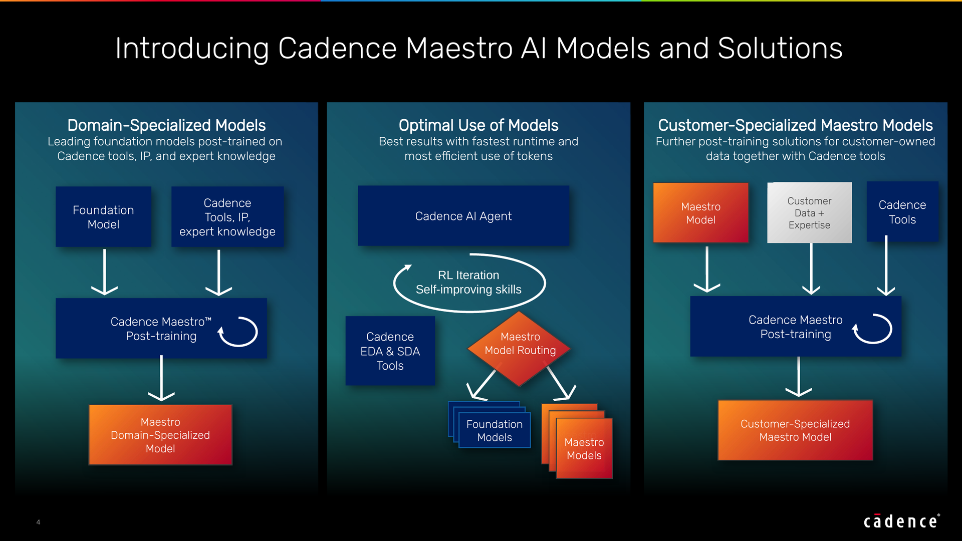
Cadence, one of the largest electronic design automation (EDA) companies, has unveiled Maestro, its new portfolio of domain-specialized AI models tailored for its chip design agents, in a press release sent just ahead of earnings. In initial results compared with general-purpose AI models, Cadence claims up to a 30% improvement in the quality of results and that Maestro effectively uses fewer tokens for the same task, with up to 5x the token efficiency. The first models “are available to select early access customers” in Q4 2026, and customers may run them on Cadence’s cloud, public clouds, or customer-controlled on-premises environments and post-train them on their own “proprietary data, designs, and workflows.” To learn more about Maestro, we spoke with two Cadence executives: Rob Knoth, senior group director of strategy and new ventures, and Paul Cunningham, senior vice president and general manager.
This approach is distinct from Synopsys’ own specialized model, GPT-Synopsys, which will run on OpenAI-hosted infrastructure, without using customer data to train the model. The models of both EDA giants, announced less than a month apart, now split on where a customer’s design data goes. Where they might not differ is why: Paul Cunningham, senior vice president and general manager at Cadence, told Tom’s Hardware Premium that agent costs have “really started to explode,” adding, “And I think the world realized so.” That makes it a natural step, he said, to move more of the agents’ iterating “into the weights of the models themselves.”
(Image credit: Cadence)
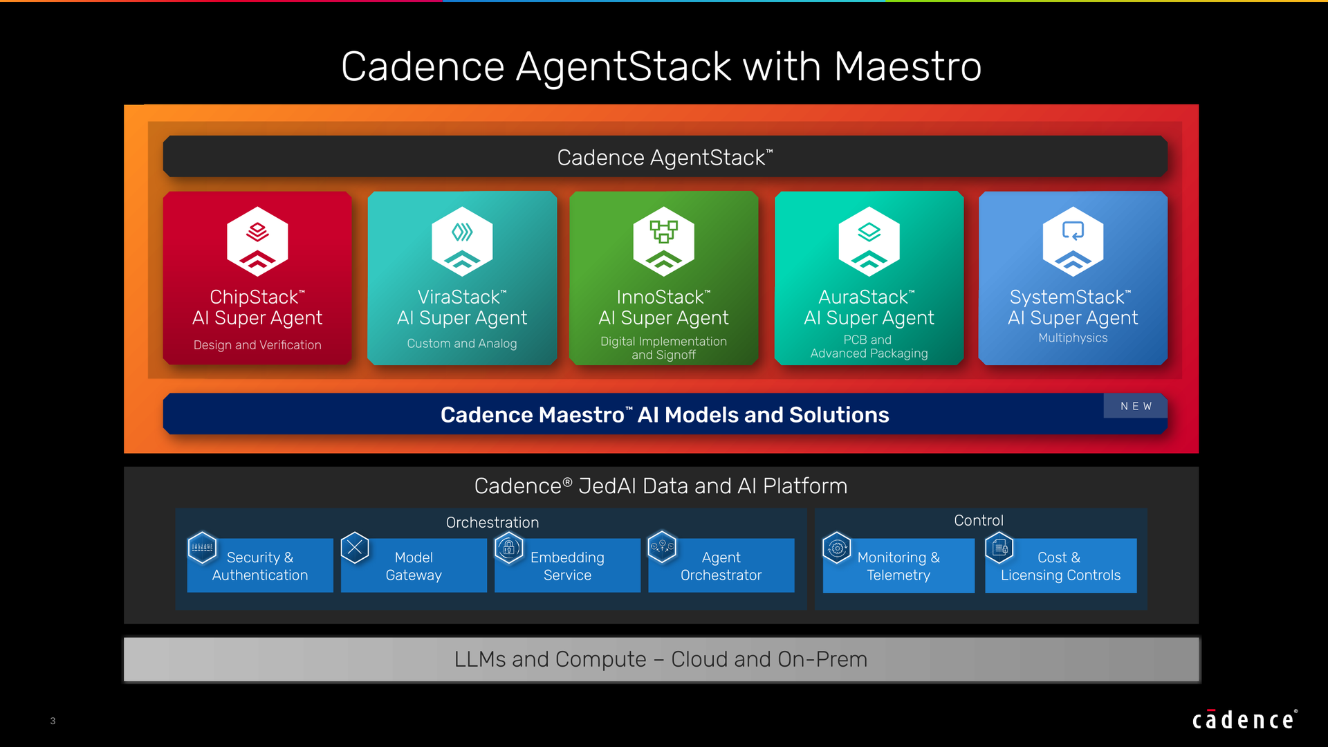
Maestro takes this step through Cadence’s AI Super Agents, which “interpret design intent, decompose tasks” and “orchestrate the Maestro portfolio with other leading frontier and open-weight models,” evaluating trade-offs to guide decisions with domain expertise. It also uses reinforcement learning (RL), where Cadence’s “deterministic solvers evaluate outputs against engineering objectives, constraints and ground truth,” and, importantly, the results feed back into the models for improvement.
The models include Nvidia’s Nemotron, and customers can run the customer-data training step themselves with Cadence’s fine-tuning harness, potentially “on their own GPUs, on their own network,” Cunningham said. He added that Nemotron, specifically, was “giving really solid results and actually improving very, very fast.”
One constant that keeps popping up with agentic EDA is the need to nail down what the numbers actually measure. In chip design, quality of results usually refers to the design’s power, performance, and area, though Cadence didn’t specify what its 30% figure measures. Both it and the 5x token efficiency figure are measured against “a general-purpose foundation model,” which Cadence told us is the open-source model Maestro started from before its training. The company wouldn’t name the foundational AI model that Maestro is derived from beyond mentioning that it is “one of the leading open source models that’s very competitive with commercial frontier models.”
Cadence credits the token savings to balancing its EDA and system design automation (SDA) “tool calls with LLM invocations.” As an analogy, Cunningham said, “You don’t need to drive to Safeway in the jet engine,” and you want to use “the right model at the right time for the right task.”
Runtime does matter, too: as Rob Knoth, senior group director of strategy and new ventures at Cadence, told Tom’s Hardware Premium in September that a tool call could take anywhere from hours to days to return a value, while the AI industry’s training loops are “used to minutes.” Efficiency could also lower costs, since Maestro use counts toward Cadence’s agent pricing, a subscription with a consumption allowance and charges for use beyond it, Cunningham said. He didn’t say whether the token savings cut a customer’s bill.
Being flexible for the customer is a key element of any solution, and for Cadence’s competitor Synopsys, this lies in Autopilot, which Synopsys says allows customers to “choose among commercial, open-source, and fine-tuned language models” across “Synopsys-managed and customer-managed deployments,” with cloud or on-premises infrastructure. For agent security, such as sandboxing, Cadence says it’s working with Nvidia on an integration with Nvidia’s OpenShell Reference Architecture, which Nvidia launched last week, naming both Cadence and Synopsys. These options can help protect customer intellectual property.
Cadence Maestro vs. GPT-Synopsys
Cadence Maestro
GPT-Synopsys
Announced
Oct. 26, 2026
Sept. 30, 2026
What it is
A portfolio of domain-specialized AI models for Cadence’s AI Super Agents
A specialized model that operates Synopsys’ tools directly
Model partner
Nvidia (Nemotron, OpenShell)
OpenAI
Models
Post-trained LLMs, trained decision models and agent skills, blended with frontier and open-weight models, including Nemotron
OpenAI frontier models
Where it runs
Cadence’s cloud, public clouds or customer-controlled on-premises environments
OpenAI-hosted infrastructure
Customer data
Customers can post-train it on their own data, designs and workflows, with Cadence’s fine-tuning tools
Customer data isn’t used to train the model
Claimed results
Up to 30% higher quality of results and up to 5x token efficiency vs. a general-purpose foundation model, the unnamed open-source model Maestro started from (initial results; measure not stated)
None disclosed
Availability
First models to select early-access customers in Q4 2026
No date; early technology engagements underway
Customers named
Socionext, Silicon Labs (Nvidia as partner), frontier AI labs
None
Pricing
Subscription with a usage allowance, then charged by use
Not disclosed; Synopsys and OpenAI share revenue under their deal
Cadence has had a busy 12 months with customers and agents alike. During Cadence’s July earnings call, CEO Anirudh Devgan said ChipStack, its design and verification agent, “has more than 20 customer engagements,” and ViraStack, its custom and analog agent, “more than 25 customer engagements.” Socionext said just last week that it was applying InnoStack. Silicon Labs has also credited ChipStack with accelerating debugging, and both companies say they are watching Maestro next.
Cadence's agentic consolidation began with its acquisition of ChipStack back in November 2025. In June 2026, the company claimed that its agent had reached Level 5 autonomy, which we explored in detail. In September, Knoth teased Maestro’s ingredients to Tom's Hardware Premium a month early, two days before the GPT-Synopsys announcement: “reinforcement learning loops, domain-specific post-training of open-weight models, model routing.” Maestro is now sitting under all four super agents, targeting a similar year-end window to Synopsys’ Autopilot; the table below has the full timeline.
Done; co-founder Kartik Hegde now leads Cadence’s core AI research group
February 2026
ChipStack AI Super Agent
Up to 10x productivity for coding designs and testbenches, test plans, regressions and debug
In early access since launch
April 2026
ViraStack (custom and analog), InnoStack (digital implementation) and AgentStack (head agent)
—
Socionext is deploying InnoStack in production; others not stated
June 2026
ChipStack at Level 5, with Nvidia’s Nemotron and OpenShell
Over 40x faster RTL validation cycles in Nvidia’s deployment
Level 5 and AgentStack due to early-access customers in the second half of 2026
July 2026
AuraStack (PCB and advanced packaging)
Up to 2x faster time to market and 15x higher productivity
Available on Cadence’s Millennium M2000 supercomputer; Nokia is deploying it (Oct. 21)
September 2026
ChipStack RTL Generation Agent
An average of 24% less area and 18% less power than pure foundation-model code, in early evaluations
Due to select early-access customers in Q4 2026; early collaboration with Honda R&D
Oct. 26, 2026
Maestro AI Model Portfolio
Up to 30% higher quality of results and up to 5x token efficiency vs. a general-purpose foundation model, in initial results
First models available to select early-access customers in Q4 2026; about a dozen engagements
This rapid pace of progress means that a clear distinction has to be made between early access and general availability. Both Cadence and Synopsys can point to customer engagements, and, at least in the latter’s case for the AgentEngineer portfolio and Autopilot platform, general availability remains a goal by year’s end; Cadence hasn’t given a general availability date for Maestro. For GPT-Synopsys, though, only “early technology engagements are underway,” according to its partners. The platforms and agents remain works in progress.
For Maestro, Cunningham hopes for “more case studies, more quantifiable benefits” through Q4. The real story, as he aptly put it, is that “we’re going to bring agents and agentic AI natively into our vertical, not that our vertical is going to get embedded into general-purpose agents.” Only customer results on real workflows will test Cadence’s 30% number, but going by what both companies have shown so far, their own early figures are extremely promising and exciting for the EDA industry.
Intel and AMD have spent decades competing for the processors inside PCs and data centers, but the rivalry hasn't stopped the two companies from working together when their interests align. And now, Intel CEO Lip-Bu Tan has reportedly discussed potential areas of cooperation with AMD chief Lisa Su, adding another possible partnership to the mix as Intel tries to regain its footing in the semiconductor industry.
According to a recording (embedded below) of Tan’s October 24 fireside chat with Chinese American Semiconductor Professional Association (CASPA) President Jimmy Cheng, the Intel CEO outlined his plans to rebuild the company’s CPU business, develop chips tailored to specific customer workloads, and attract more customers to its foundry operations. However, Tan did not publicly detail the reported areas of potential cooperation with AMD CEO Lisa Su.
Intel has traditionally built its business around its own processor roadmaps, but Tan says the company needs to be more flexible as customers look for silicon designed for particular workloads. He pointed to Intel's Xeon processors as one area where that approach is changing, alongside continued development of GPUs and accelerators.
"We have to reclaim the leadership in CPU. That is something that I am very determined to do." Tan said.
He also described a change in how Intel approaches customization. "Intel is so proud they never want to modify for customer needs," he said. "I'm modifying it for customer needs, and so that, I think, to me, is a fast-growing area, and I'm double, triple down on it."
The strategy extends beyond conventional CPUs, with Tan identifying application-specific integrated circuits (ASICs), co-packaged optics (CPO), physical AI, and advanced packaging as potential growth businesses. He wants two or three of these areas to eventually contribute around 10% of Intel's revenue each.
Intel's foundry business is another major part of Tan's plans. He said the company's 18A manufacturing process had reached volume production, while development of its next-generation 14A process was progressing strongly. Intel has already released version 0.5 of the 14A process design kit (PDK), which provides chip designers with the technical information and tools needed to develop products for the process.
Tan said version 0.9 was coming next, followed by version 1.0 for volume production in early 2027. "We have multiple customers [who] really want us to really scale their business," he said, referring to interest in Intel's foundry services.
However, Intel did not identify those customers or disclose the size of any potential manufacturing orders during the discussion. Notably, in January,Intel had two prospective customers evaluating 14A test chips, with firm supplier decisions expected during the second half of 2026 and the first half of 2027. Tan also described foundry manufacturing as a business where trust matters as much as technology. Customers hand over wafers that will eventually become products on which their own revenue depends, making missed deadlines or manufacturing problems costly. "The moment we take on the foundry, take on the wafer is a lot of responsibility to make them successful," he said.
He recalled one customer who had waited six to eight months hoping he would become CEO before presenting 15 areas where Intel had fallen short. Tan said he addressed the problems individually, after which the customer agreed to deepen its relationship with Intel.
That said, the prospect of further cooperation would not be entirely new. In October 2024, Intel and AMD established the x86 Ecosystem Advisory Group alongside other technology companies to coordinate improvements to the x86 instruction set architecture and make it easier for hardware and software developers to support both companies' processors.
That cooperation has since moved into AI software. Last week, it emerged thatAMD was integrating its ZenDNN optimizations into Intel's open-source oneDNN library, bringing the companies' CPU optimization work for PyTorch AI inference under a common software path. The companies have also worked together on Advanced Matrix Extensions and other x86 capabilities through the advisory group, showing that they cooperate on shared technologies while continuing to compete for customers. For now, however, neither company has announced a new agreement arising from the discussions.
Export controls have kept ASML's most advanced EUV lithography machines out of China. Instead, the country's chipmaking industry has relied on less-capable deep ultraviolet (DUV) lithography machines. By using multiple exposures on critical chip layers, these older machines are still capable of producing performant silicon. However, as multiple patterns are applied there are more chances for defects, longer manufacturing times, and higher bills. We spoke to experts like Chris Mack, co-founder and CTO of semiconductor firm Fractilia, to find out how much further DUV can go.
For years, extreme ultraviolet (EUV) lithography has been seen as China’s biggest choke point in the country’s attempts to build cutting-edge chips. The machines, made exclusively by Dutch manufacturer ASML, use 13.5nm-wavelength light to print some of the most intricate features found on modern processors.Sales of ASML’s EUV systems are subject to export restrictions, forcing Chinese manufacturers to squeeze ever more out of older deep ultraviolet, or DUV, lithography instead. The EUV gap alone between China and the West is atleast half a decade, according to some analysts.
But even without access to EUV machines, China has gotten surprisingly far in recreating what it offers through existing technology.
Teardowns of Huawei’s Mate 60 Pro in 2023 found the phone’s Kirin 9000S processor had been made by SMIC using a second-generation 7nm-class manufacturing process without EUV. More recently,analysis of Huawei’s Kirin 9030 found SMIC had pushed its DUV-based process closer still to the density associated with 5nm manufacturing – although it continued to lag behind the leading processes used by TSMC and Samsung.
Multiple patterning
The trick is multiple patterning. Rather than trying to print an overly intricate chip layer in a single pass, Chinese manufacturers are dividing up the complex design into several simpler patterns. Repeat the process enough times and you can etch up something approximating the proper layer you intended.
The trick works. But according to lithography expert Chris Mack, co-founder and CTO of Fractilia, asking whether a chip can be made without EUV overlooks the trade-offs manufacturers make in order to do it.
“When this transition first began, what everyone in the industry said as conventional wisdom is that cost-wise, three exposures on a 193 immersion tool cost about the same as one exposure on an EUV tool,” Mack said in an interview with Tom’s Hardware Premium. “At three, it was about even,” Mack explained. “But as soon as you hit four masks – 193 masks being replaced by one EUV mask – then EUV became more cost-effective.”
It’s also likely to produce a higher quality product with fewer defects. Each time a wafer is patterned, that new pattern has to line up perfectly with everything that’s already been etched beneath it. The more individual exposures needed to produce a single layer, the more opportunities there are for things to go wrong. “If you have, say, four 193 masks, you've got all those different overlays, and you've got all these different process variations that start to accumulate,” Mack said.
Chip designers can try and avoid that by leaving more space around features so the finished processor can actually be manufactured reliably. But that means the chip ends up bigger – and bigger chips become expensive very quickly. Making each die larger means fewer fit on every wafer, and wafers cost a lot of money – tens of thousands of dollars each.
“You don't sell wafers, you sell die,” Mack said. “The question is: how many die can I fit onto that wafer, and how many of those die yield, and therefore how many chips can I sell per wafer?”
The efficiency gap
There is some evidence of what that efficiency gap can look like in practice – albeit in memory rather than logic chips. In a June report, Morgan Stanley estimated that Chinese DRAM manufacturer CXMT was producing only around one-third as many bits per wafer as Western competitors. The analysts believed the older process node only accounted for around a third of that shortfall, but said access to lithography was a “hard ceiling” on Chinese memory development. “For advanced logic chips, in theory there could be other innovations to engineer around EUV, but they are not likely to be very efficient and effective,” said Douglas Fuller, a researcher at Copenhagen Business School, in comments to Tom’s Hardware Premium.
It is also why claims that China has reached a particular semiconductor process “node” need to be treated with caution. “If somebody says it's X node – the seven nanometer node, the five nanometer node, the three nanometer node – these words almost have no meaning,” Mack said.
That can be seen in SMIC’s latest chips. Reporting suggests its N+3 process representsmeaningful progress towards 5nm-class manufacturing – but the actual measurements show it remains significantly less scaled than established 5nm processes from Samsung and TSMC. That doesn’t mean DUV has reached the end of its useful exploitation.
Stretching DUV's efficacy
Micron is an example of how far DUV can be stretched, producing competitive DRAM chips using DUV, multiple patterning and tight process control. Its 1-alpha generation of chips wasdeveloped without EUV. “They pushed 193 farther than any of the other memory makers did,” Mack said. “They were able to make very competitive chips with 100% 193 compared to Samsung and Hynix making them with many layers of EUV.”
Morgan Stanley believes CXMT’s planned move to 1-alpha DRAM – which it wants to use for HBM3e – is achievable without access to EUV, citing Micron as evidence. Indeed, “by the end of the decade, advanced packaging will allow firms to use DUV to produce the latest generations of DRAM,” reckons Fuller.
Micron also designed its products around the manufacturing technology available to it, rather than simply trying to recreate an EUV process on older equipment – something which could be a useful lesson for Chinese manufacturers. “If the entire ecosystem of 193 immersion were available to China,” Mack explained, “then they could probably push a long way with 193 multiple patterning, especially if they optimise designs for the fact that they're going to be using that.”
But Micron was making memory, whose highly repetitive structures make close co-ordination between chip design and manufacturing easier than it is for the much more complicated logic processors found in phones and computers.
“Memory is a lot easier than logic,” Mack said.
And even Micron eventually concluded that EUV was worth using. Its newer 1-gamma DRAM processuses EUV lithography, with Micron saying the technology helps it achieve more than 30% greater bit density per wafer than its preceding 1-beta generation.
EUV is hardly a magic wand, either. Mack points to stochastic effects – tiny random variations caused by the small number of photons involved in an exposure – which mean manufacturers can improve pattern control by increasing the EUV exposure dose. But it also pushes the cost back up quickly.
Because of that, Mack believes there is ultimately a limit to how far multiple patterning can economically substitute for EUV. “I would be hard pressed to really believe that a three nanometer or a two nanometer node is going to be economically viable without EUV,” he said.
That doesn’t mean Chinese chipmakers simply hit a technological wall and stop. They can keep pushing DUV while accepting larger dies, poorer yields, longer manufacturing times – or some combination of all three.
They can also throw capacity and money at part of the problem. Morgan Stanley assumes CXMT remains stuck on its 1-alpha process without EUV, yet still increases its share of global DRAM bit supply from 14% in 2026 to 16% in 2028 simply by building more greenfield capacity. The bank also expects China’s AI chip self-sufficiency to rise from 42% in 2025 to 70% by 2030 through new advanced-node capacity, improving yields and heavy state support – while EUV, HBM and advanced software leave a persistent gap. And so without EUV, the experts reckon China can only get partway to bridging the gap with the West. ““I would be hard pressed,” said Mack, “to really believe that a three nanometer or a two nanometer node is going to be economically viable without EUV.”
TSMC, the world's largest contract chip manufacturer, is seeking alternative machinery without rare-earth components to reduce its dependence on China-dominated materials and avoid disruptions to factory operations caused by the country's export controls. According to a Reutersreport on October 22 citing people familiar with the matter, the Taiwanese company has begun approaching its equipment suppliers to explore whether they can provide factory automation equipment equipped with motors that don't require rare-earth materials.
TSMC supplies the extremely powerful Nvidia chips that are facilitating the AI boom. It also manufactures chips for Apple, Broadcom, Qualcomm, and numerous other tech and automotive companies. The company operates enormous, highly automated semiconductor fabrication plants. These factories use industrial machinery that relies on electric motors with powerful permanent magnets made from rare-earth elements such as neodymium, dysprosium, and terbium.
According to the U.S. Geological Survey (USGS), China accounts for roughly 70% of global rare earth mining. The International Energy Agency (IEA) says China also controls around 90% of refining and approximately 95% of the finished permanent magnets found in TSMC’s machines, giving Beijing a quasi-absolute monopoly over one of the most critical technology supply chains. In April 2025, the country placed seven medium and heavy rare earths and the magnets made from them under export controls, requiring exporters to seek case-by-case approval and export licenses, thereby choking shipments to manufacturers across the U.S., Europe, and Asia, including TSMC.
China expanded the controls on October 9, 2025, to include five additional rare earths, processing technology and equipment, and even products manufactured outside the country that contain more than 0.1% Chinese-origin rare earths, or are made using Chinese processing technology. It later suspended the October expansion for one year, until November 10, 2026. This has now been extended for an additional 90 days.
TSMC’s moves aim to reduce the risk that these controls will hinder production at its factories. Even with all other raw materials and machinery required to manufacture its chips, shortages of specialized motor components could complicate the maintenance, repair, or expansion of its production equipment. Several technological approaches allow motors to avoid rare earth magnets. Conventional induction motors, for example, generate torque using electromagnetic induction rather than permanent magnets. Switched-reluctance motors are another option, while some permanent-magnet motors can use ferrite magnets instead of rare-earth magnets. However, these technologies typically involve different trade-offs in efficiency, size, power density, precision, and control requirements.
Meanwhile, the rest of the world is undertaking the painstaking, drawn-out task of building a rare-earth supply chain outside China. Taiwan is reportedly pursuing domestic rare-earth production capabilities in collaboration with the United States, with both countries confirming their intent to reduce reliance on Chinese rare-earth and critical-mineral supply chains.
Taiwan's government is supporting the Industrial Technology Research Institute (ITRI) in establishing a pilot production line within three years that could supply about 50% of Taiwan's domestic rare-earth demand. Meanwhile, the U.S. is “working with Taiwan and other partners to develop alternative sources of supply, expand processing capacity and build more resilient supply chains,” according to the report. In February 2026, the Trump administration announced plans to create a $12 billion critical minerals stockpile to offset supply chain risks from China.
Intel on Wednesday announced that it had started installing production tools at its Fab 62 in Arizona, and the fab is on track for mass production by late 2028. The company also reported progress on its Ohio One manufacturing complex and confirmed that it has integrated High-NA EUV lithography into high-volume manufacturing (HVM). Meanwhile, Intel continues to invest in its leading-edge process technology R&D, advanced packaging, and photomask production capabilities in the U.S., which puts the company ahead of the competition.
"There is an important difference between technologies made in America and technologies that are truly American-made," wrote Naga Chandrasekaran, executive vice president and chief technology and operations officer, Intel Foundry. "The difference lies in the research and development process that transforms ideas into manufacturable technologies."
Fab 62 to begin operations in 2028
Intel completed construction of its Fab 62 shell some time ago; now it is time for the company to begin installing production tools, which is what it is doing now. Intel expects the new facility to become operational before the end of 2028, although it has not disclosed when it intends to begin high-volume production or which nodes it will produce.
(Image credit: Intel)
Intel has not officially assigned Intel 14A to Fab 62, although the facility has been discussed as a potential manufacturing site for the node. Meanwhile, there is an important distinction between Intel's original plans for Fab 62 and its current commitments. When Intel announced Fab 52 and Fab 62 in Arizona, it said the two facilities would manufacture its most advanced process technologies, including Intel 20A (2nm-class) and 18A (1.8nm-class). Intel subsequently designated Fab 52 for Intel 18A manufacturing. Yet, Fab 62 remains unassigned.
Given Intel's manufacturing process roadmap disclosed earlier this year, Fab 62 will be able to make chips on 18A, 18A-P, and 14A nodes. Intel currently manufactures Intel 18A chips at the neighboring Fab 52, whereas Fab 62 could potentially accommodate either additional Intel 18A capacity or the company’s next-generation Intel 14A process technology. However, Intel has yet to confirm its plans for the facility.
The facility will become Intel's Fab 62, the sixth high-volume semiconductor manufacturing fab at its Ocotillo campus, which has served as one of the company’s primary production sites for decades.
Intel has also not revealed Fab 62's planned wafer processing capacity, or the amount of capital expenditures required to complete the facility. Nevertheless, the installation of production equipment indicates that the project has progressed beyond construction of the building itself. The new fab will expand Intel’s manufacturing footprint in Arizona, where the company already produces leading-edge processors and operates advanced packaging, assembly, and testing facilities.
Intel confirms High-NA EUV insertion into mass production
Another noteworthy disclosure concerns Intel's deployment of High-NA EUV lithography. Intel was the first chipmaker to install a commercial High-NA EUV scanner at its D1X fab near Hillsboro, Oregon, and subsequently integrated the tool into high-volume manufacturing to produce its Panther Lake and other chips.
The Gordon Moore Park at Ronler Acres in Oregon is where Intel develops its most advanced logic process technologies and initiates volume production of the latest processors. Usage of High-NA EUV to produce select tiles for Panther Lake CPUs at D1X is a natural fit for the development fab, as it helps Intel to better understand how these lithography systems work. Meanwhile, it seems (though Intel has not explicitly confirmed) that, for now, High-NA EUV scanners are used to produce the same circuits as Low-NA EUV machines, so the use of next-generation lithography systems does not necessarily provide significant advantages over existing litho scanners.
Ohio One reaches another construction milestone
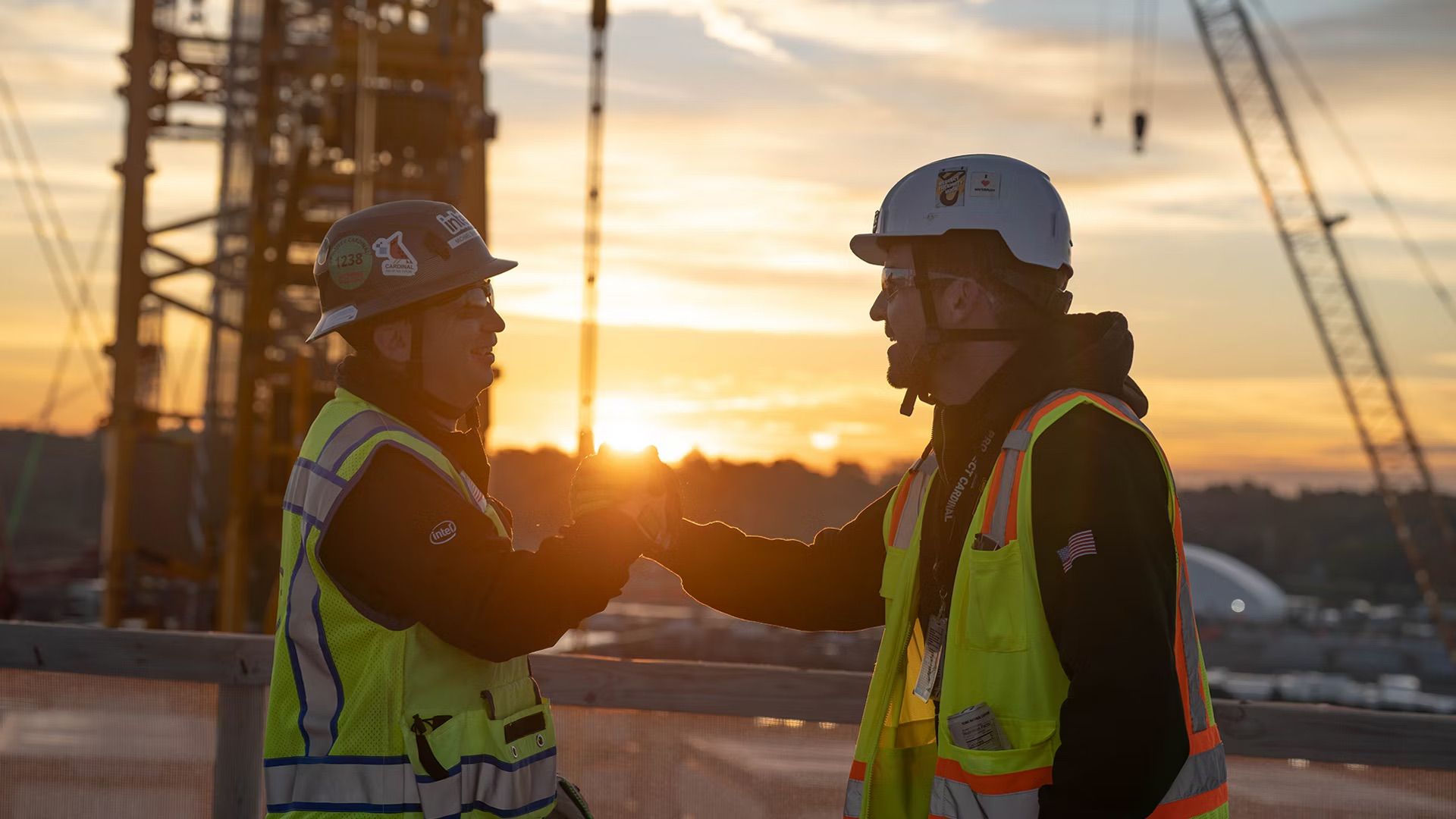
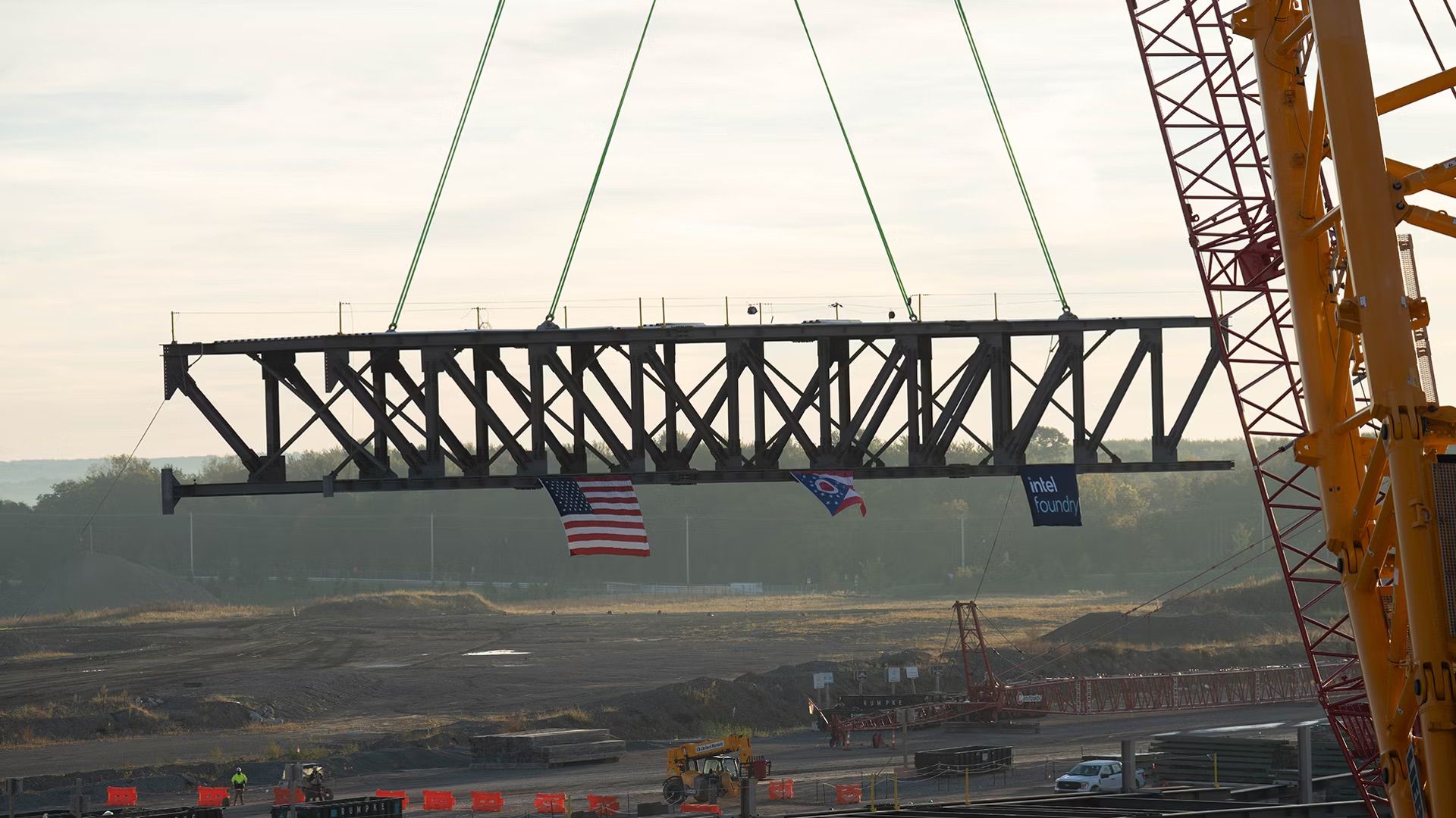
Intel has also made progress with its 'Ohio One' manufacturing complex in New Albany, Ohio. Construction workers recently installed the first major structural truss at the site's first semiconductor fab, which represents a milestone in the development of the company's manufacturing operations in the state. The project is clearly an important part of Intel's long-term strategy to expand domestic production of chips using leading-edge process technologies for years to come.
(Image credit: Intel)
Unfortunately, Intel did not provide an updated construction schedule for Ohio One or disclose when the first fab is expected to begin operations. Intel also did not reveal which process technology the facility will eventually use or the estimated manufacturing capacity it will provide. Therefore, while construction continues, which is good news, the announcement does not clarify exactly when Ohio One will contribute to Intel's output.
Other investments across the U.S.
In addition to leading-edge manufacturing capacity in the U.S., Intel continues to invest in advanced packaging technologies. Oregon serves as the company's main research and development center for advanced logic and 3D interconnect technologies, while Arizona hosts advanced packaging R&D, assembly, and testing operations. Intel uses its site in New Mexico to produce its complex multi-chiplet processors relying on advanced packaging methods — starting with modest EMIB and all the way to next-generation EMIB-T and Foveros technologies.
(Image credit: Intel)
Also, Intel recently broke ground on a new photomask manufacturing facility in Santa Clara, California. The new facility will be an important part of Intel's supply chain in the U.S., as the company will be the only chipmaker in America to develop and produce chips using leading-edge nodes completely in the U.S. (both Samsung and TSMC currently lack leading-edge process R&D in America; they do not run their own photomask shops in the U.S., and Samsung has abandoned its plan to build an advanced packaging facility in Texas). Of course, Intel critically depends on tools from Europe and materials from Japan, but even as its major rivals invest hundreds of billions in their U.S. production capacity, Intel remains ahead.
To highlight its American supply chain, Intel disclosed that its U.S. operations involve more than 4,500 suppliers across 49 states, as its annual domestic expenditures exceed $29 billion. The company stressed that domestic semiconductor leadership requires not only wafer fabrication capacity but also research, process development, advanced packaging, and a comprehensive supply chain.
Elon Musk says ASML and other critical semiconductor equipment suppliers have expedited shipments for the ambitious Terafab semiconductor manufacturing facility, supporting his aggressive timeline for the joint megaproject between Tesla and SpaceX. He made the announcement during a live broadcast of SpaceX's Q3 2026 earnings call on X yesterday, October 20. Musk also said the company is targeting volume chip production at the project's primary facility in Gibbons Creek, Texas, by the third or fourth quarter of 2028, emphasizing that the timeline is highly aspirational and carries "big error bars."
"These are very aggressive dates, and we're very appreciative of ASML and all of our other suppliers in accelerating equipment deliveries in order to achieve this outcome," said Musk, CEO of both companies behind Terafab. SpaceX plans to manufacture its first experimental test chip at its research fabrication facility in Austin, Texas, around Q2 2027.
Aside from Terafab, Musk also outlined near-term ambitions for his AI companies during the broadcast, saying he expects them to have 2.5 to 3 gigawatts (GW) of computing capacity active by the end of 2026. He also stated he is highly confident about bringing an incremental 10 GW online in 2027, saying he "would be surprised" if they do not hit a total of 13 GW of AI compute by the end of 2027.
Meanwhile, the next-largest project by planned capacity, the now-restructured 10 GW Project Stargate, was expected to reach full capacity in the 2030s. Meta's 5 GW Hyperion also has a similar timeline. To achieve the 13 GW milestone, Musk revealed that SpaceX and xAI are aggressively procuring upcoming next-generation NVIDIA architecture. He announced plans to get a massive 440,000-GPU Nvidia "Vera Rubin" training cluster online by the end of Q2 2027.
Shifting back to Terafab, Musk also boasted that once fully scaled and operational, the sheer commercial value of Terafab's advanced chip output will place it within the top 20 global country GDPs from a single physical building. For context, the 20th country on the list is Switzerland, with a GDP of around $1.14 trillion. The facility is a planned multi-billion-dollar, vertically integrated chip factory in Texas, with an ambitious goal of manufacturing 1 terawatt (TW) of AI computing power per year. Terafab will fabricate logic, memory, and advanced packaging internal architectures in one place. The project's massive planned output has mandated various collaborations across the semiconductor supply chain. Terafab will utilize traditional extreme ultraviolet (EUV) lithography systems utilizing Intel's 14A manufacturing node technology.
Intel officially joined the Terafab venture in April 2026 to help co-develop and refactor silicon fabrication technology, providing access to its state-of-the-art 14A manufacturing process. ASML, the world's sole commercial supplier of the $400 million EUV lithography systems required for high-volume, leading-edge chip production, is perhaps the project's most critical partner. Terafab's first EUV tool was reportedly slated for delivery in mid-2027, according to unofficial sources. It remains unclear if this is the expedited timeline Musk referred to in the broadcast.
Other major suppliers include American equipment manufacturers Applied Materials, Lam Research, and KLA Corporation, as well as Japan's Tokyo Electron. These companies will provide front-end processing, metrology, and process control machinery. Tesla and SpaceX are also in talks with about 10 South Korean equipment makers, including Hanmi Semiconductor, known for advanced packaging equipment, and HPSP, a high-pressure hydrogen annealing equipment manufacturer, as well as firms providing specialized piping components and process valves.
Musk's announcement says that several of these suppliers are expediting supply to Terafab, even as capacity remains tight across the semiconductor supply chain. The facility, which aims to mitigate future shortfalls of cutting-edge AI processors from external foundries like TSMC, will supply the chips for Musk's xAI clusters, self-driving vehicles, Optimus humanoid robots, and SpaceX's orbital AI data center, as well as the broader AI industry.
However, many experts have questioned the validity of Musk's 1 TW Terafab ambition. For context, research firm Gartner estimates the total global AI-optimized data center capacity is roughly 44 GW as of late 2026, 4.4% of Terafab's planned output. Although global AI computing capacity has grown by roughly 3.3x to 3.4x per year since 2022, according to EpochAI.
Three contract workers died, and one more is in intensive care after an accident at the construction site for TSMC’s 2nm Fab 22 in Kaohsiung, Taiwan, reports Taiwan’s Central News Agency. The Southern Taiwan Science Park (STSP) Bureau suspects the cause was a broken bolt on a steel connection plate that sent the workers and steel components tumbling. Steel hoisting on the project has been halted, and the STSP has sent labor inspectors to investigate. The accident is not the first of its kind but rather follows at least a half dozen others since September 2024 at TSMC construction sites in Taiwan, according to local reports. Each of those earlier accidents killed one worker.
Local police said that the men were welding a steel beam on an upper floor and fell with it, while the STSP said the workers were performing steel-structure hoisting and installation when a third-floor connection-plate bolt apparently broke.
10 emergency vehicles were sent to the site with 22 personnel, and all four men involved in the incident were taken to the hospital. On-site medical staff gave first aid, but three of the workers died despite resuscitation efforts, and the fourth was moved to intensive care. The workers were employed by a contractor working on the fourth phase of the complex’s construction, and TSMC said the area was within that contractor’s scope of work.
According to the report, TSMC stopped the related construction work on its own and is working with authorities and supervising the subcontractor’s follow-up.
The Fab 22 complex, located in Kaohsiung’s Nanzi District, is part of the science park and is being built to accelerate 2nm manufacturing. TSMC entered high-volume 2nm, or N2, manufacturing in the fourth quarter of 2025, including at Fab 22. The complex has five phases planned, with a total investment TSMC puts at more than NT$1.5 trillion, or about $46 billion. The accident happened on the construction side, not in a producing fab. Kaohsiung’s deputy mayor said construction on Phase 4 began in August 2025, with operations expected in the fourth quarter of 2027.
Business Today reports that TSMC fab construction has increased, from four fabs a year in 2017–2024 to nine a year in 2025 and 2026. The deaths come as the company plans for 13 new leading-edge and advanced-packaging fabs in Taiwan, with company-wide capex of $60 billion to $64 billion this year.
The faster pace has encouraged the addition of a contractor’s safety record as a weight in selection and a plan for a Taiwan Semiconductor Construction Engineering Safety Association with construction partners. TSMC Chairman C.C. Wei said at last year’s shareholders meeting that safety cannot be compromised, and the company’s 2025 annual report said it will keep investing in fabs across several locations in Taiwan “with a strong emphasis on construction site safety.”
Cliff Hou, TSMC senior vice president and deputy co-COO, told Business Today that increased worker count and overlapping construction have raised the risk, requiring careful supervision, and that TSMC’s contractor lost-time injury rate had fallen about 42% from last year’s high as of late May, when the publication toured the Nanzi site to see the overhaul. It’s too early to call the program a failure, with the cause as yet unknown.
The accident comes less than a week after an explosion killed two people at Intel’s chip plant in Israel, though that was an operating fab rather than a construction site. Both accidents come as chipmakers race to meet demand, with global chip sales passing $1 trillion through August, according to the Semiconductor Industry Association.
The STSP’s findings will determine what penalties, if any, will fall under Taiwan’s Occupational Safety and Health Act, while it assists the victims’ families. No date has been given at this time for that or for the Phase 4 steel hoisting restart. Nor has TSMC commented on any schedule impact.
Intel has asked the Federal Communications Commission (FCC) to make an exception for the automated guided vehicles (AGVs) that the company uses to transport the sensitive silicon wafers and other materials, containers, and supplies needed to make the most advanced chips in its fabs. According to Bloomberg, the American chipmaker fears that its AGVs would fall under the blanket prohibition against foreign-made robots after they were added to the FCC’s Covered List.
AGVs are niche machines that chip fabs use to transport materials and supplies between tools and sections of the fab, helping ensure that the cleanroom conditions required for each manufacturing process are maintained. This makes them critical equipment for U.S. semiconductor manufacturing, but, apparently, there are no suitable domestic alternatives for these devices at the moment. Intel’s current fleet of AGVs requires continuous maintenance, including software and firmware updates, and if it’s forced to find a local supplier for its AGVs, the company says that it would take years, crippling the United States’ chipmaking efforts.
The biggest AGV suppliers are Japanese companies like Murata Machinery and Daifuku Co., while a few smaller businesses from South Korea and Taiwan are also trying to break into the market. It’s unclear why these companies haven’t applied for a conditional approval yet, which would allow them to continue selling these products in the U.S. while also promising Washington that they’ll set up a manufacturing base in the country. This is something that Netgear has already done, allowing it to continue selling its foreign-made routers despite being an American company.
Intel says that it remains unclear if updates to its AGVs would break compliance with the FCC, and that it’s asking the agency to issue a conditional waiver “out of an abundance of caution to ensure the ongoing operation of these specific AGV units.” While Team Blue is the only company concerned about AGVs at the moment, other chip manufacturers would likely need a similar waiver in the near future, especially as they build more fabs in the U.S. This includes TSMC, which is planning to build 12 more fabs and four packaging facilities in Arizona, Samsung, with its new Taylor, Texas, fab, and even Elon Musk’s Terafab, which has already begun construction.
Washington has been using the FCC to force companies to invest in American manufacturing. Its blanket bans on foreign-made products like drones and routers have affected some of the biggest brands in the U.S., including DJI and TP-Link. While these bans do not outright ban the sale of all products made by these companies, especially those that have already been approved before, they make it impossible for them to introduce new products and even release software updates to their existing product line. The FCC eventually walked back on the software update ban, but they still would not be able to register new products unless they build them in the U.S.
Taiwan is expanding its list of controlled exports to include AI servers and the latest chips in a move to align its policies with the U.S.’s trade bans. Bloomberg reports that after the export controls take effect, anyone caught smuggling these items will be criminally charged under the Foreign Trade Act, which carries a penalty of up to five years in prison and/or a fine of around $92,500.
“Going forward, some of our measures on controlled items will correspond to American ones because we have made quite some commitments in the Agreement on Reciprocal Trade,” Taiwan Minister of Economic Affairs Kung Ming-hsin said. The two parties signed the trade deal earlier this year, which saw the U.S. cutting tariffs on Taiwanese goods down to 15% in exchange for direct investments in the U.S. tech industry, among others.
The U.S. has long been trying to stamp out the smuggling of advanced Nvidia chips into China. One of the biggest cases that U.S. authorities have prosecuted so far includes three Super Micro employees, including its co-founder Yih-Shyan “Wally” Liaw, who are accused of smuggling $2.5 billion worth of AI servers. A few months after this revelation, Taiwanese authorities raided Super Micro’s Taipei offices in connection with the Nvidia B300 smuggling probe, which eventually led to the indictment of nine individuals related to the case.
Since Taiwan doesn’t treat AI chip exports to China as a crime before this new set of export controls is enacted, people violating the chip bans would have to be charged under other laws. This is what Singapore did when it arrested suspected Nvidia AI GPU smugglers — because it doesn’t have a law that prohibits the export of advanced AI chips to China, it instead charged the individuals with fraud and money laundering.
The expansion of the Foreign Trade Act will be one of the strictest measures that the Taiwanese government has put into place against exports to China, which is something that it has been considering earlier this year. This move will likely please Washington as it pressures other countries to take more steps in its controlling the flow of advanced AI chips into China. However, it will also likely provoke Beijing, which has already condemned Taipei after it applied export restrictions on Huawei and SMIC last year.
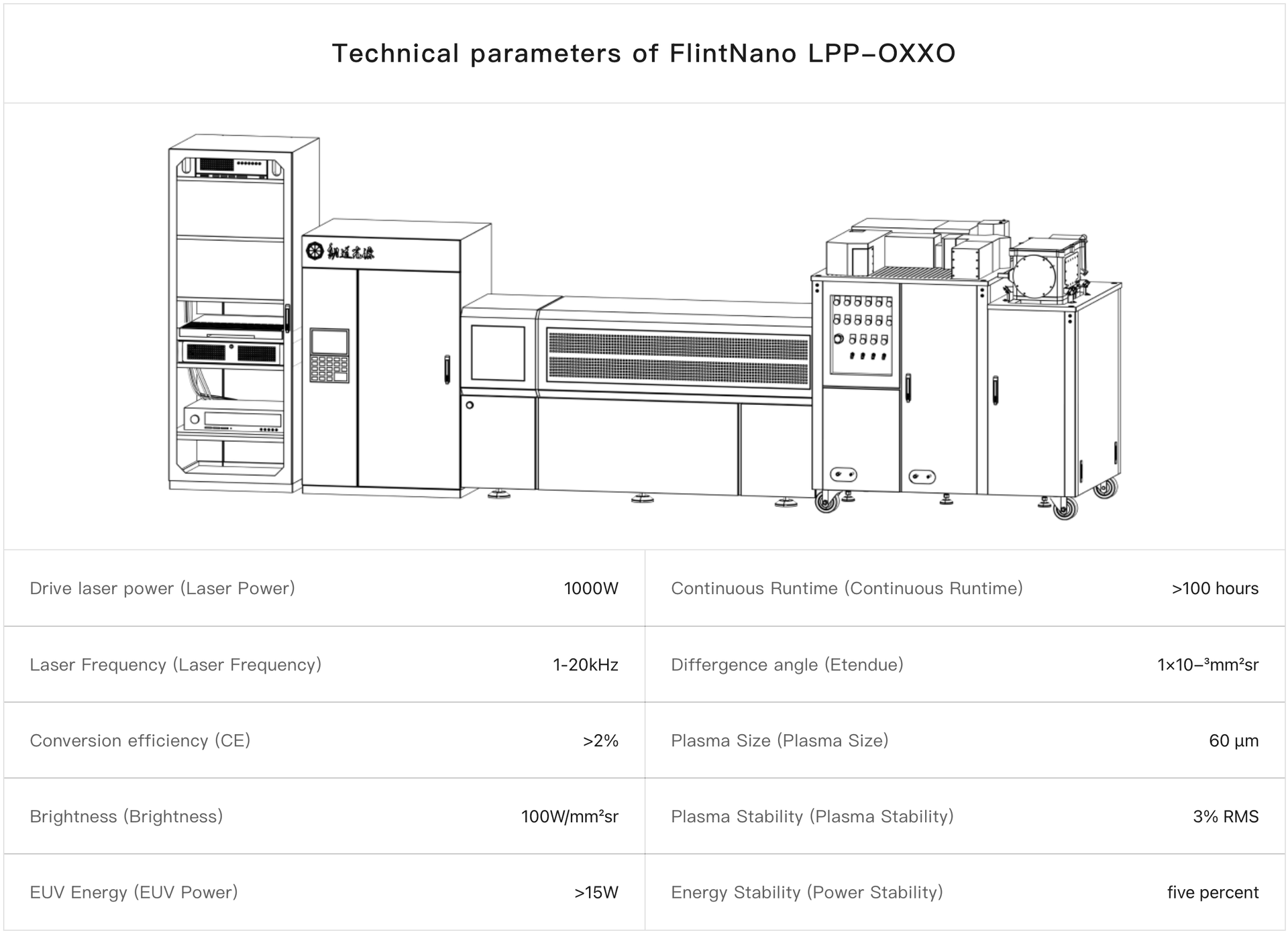
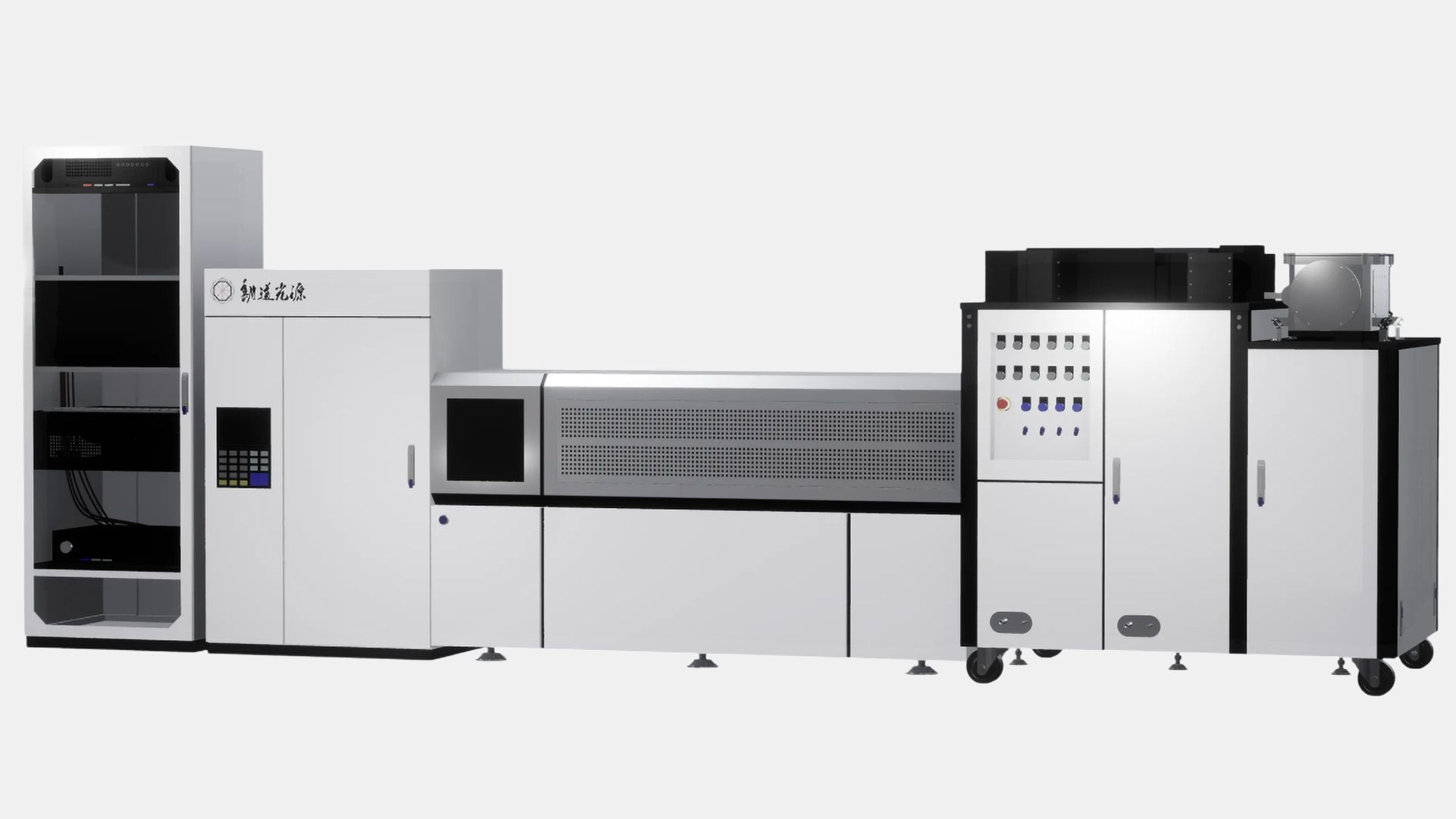
Being unable to procure EUV litho tools from ASML, China must develop such systems locally, so from time to time we learn about an EUV-related 'breakthrough' in China that will turn into an actual EUV scanner over the following several years. This week, Chinese startup Langdao Silex demonstrated a prototype extreme ultraviolet (EUV) light source with over 15W of output power, 90% domestic components, and decent uptime. The company will need another three to five years to commercialize its technology, reports TrendForce, citing various sources. Yet, a light source alone does not make an EUV scanner.
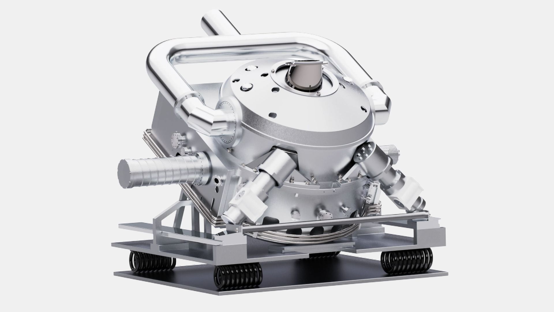
Langdao Silex, which was established in 2024 by Tsinghua University's Gas Discharge Plasma Laboratory alumni, demonstrated its EUV light source prototype at the 26th China International Industry Fair in Shanghai, for obvious reasons, without lighting it up. Just like modern light sources from ASML, the company's low-power FlintNano LPP-OXXO system uses laser-produced plasma (LPP) technology that produces EUV radiation by bombarding tiny heated metal droplets with high-energy laser pulses to create extremely hot plasma. The system features a 1,000W driving laser (presumably a CO2 one) with an operating frequency of 1 kHz – 20 kHz and conversion efficiency exceeding 2%. Its EUV output exceeds 15W (presumably measured at the plasma rather than at intermediate focus, as the company has not demonstrated a complete EUV collection system) while its brightness reaches 100 W/(mm²·sr). The source has an étendue of 1 × 10⁻³ mm²·sr and generates plasma with a diameter of 60 μm.
(Image credit: Langdao Silex)
According to Langdao's specifications, the FlintNano LPP-OXXO can operate continuously for over 100 hours with plasma stability of 3% RMS and EUV output power stability of 5%. These characteristics make the system suitable for semiconductor exposure experiments, although its output remains insufficient for high-volume chip production. Meanwhile, the 'over 100 hours' availability is very impressive for a pre-production light source, though we must admit that there is no way to verify the claim.
Langdao is also developing the FlintMicro-LPP high-power EUV source, which has completed proof-of-principle validation, according to reports. However, Langdao has not disclosed its output power, conversion efficiency, or operating lifetime.
On paper, Langdao's EUV source is comparable in output to some of the earliest EUV sources developed by Western and Japanese equipment makers, albeit with a major caveat: Langdao seems to measure EUV power at the plasma rather than after the collector or at intermediate focus as ASML does. ASML's early EUV demonstration equipment used approximately 10W at intermediate focus DPP sources in 2007, while Cymer's LPP sources installed in early NXE:3100 systems delivered up to 11W during wafer exposure in 2012 (note that ASML's machines are source agnostic, so some NXE:3100 prototypes used DPP sources, while others used LPP sources). By 2013, Cymer demonstrated approximately 40W at intermediate focus over extended operating periods. Meanwhile, Japan's Gigaphoton targeted 25W with its first prototype in 2013 and demonstrated 43W in early 2014. By late 2014, Gigaphoton had achieved 118W during a 10-minute test. However, since these historical figures involve different measurement conditions and operating durations, direct comparisons are vastly inaccurate.
Not quite there
Langdao Silex has not demonstrated its EUV light source in action, so all we know about it comes from the company itself. As noted, 15W power looks comparable to early EUV sources developed by Philips Extreme UV (DPP) and Cymer (LPP). Meanwhile, early NXE:3400-series machines came with 125W – 150W at intermediate focus sources, which was far from enough for high-volume manufacturing (HVM).
(Image credit: Langdao Silex)
Modern EUV lithography equipment comes with considerably more powerful sources. ASML introduced 250W-class EUV sources for commercial production in 2018 – 2019 and has since achieved substantially higher output levels. Increasing output requires more powerful CO₂ lasers, highly accurate tin-droplet generators, effective debris mitigation, durable collector mirrors, and considerably better long-term reliability.
Langdao claims that 90% of its prototype's components are domestically sourced and that most critical parts were developed in China. However, the company has not explained whether the localization figure reflects component count, value, or another metric. Furthermore, its representatives reportedly acknowledged that increasing EUV output and improving long-term operational stability are the targets to be achieved in a bid to commercialize the source.
Not an EUV scanner
Yet, even without complete EUV scanners, Langdao's source could support EUV photoresist development, mask inspection research, development of EUV collection and illumination optics, and eventually experimental exposure testing.
Developing a complete EUV lithography scanner will require further advances in EUV collection and illumination systems, high-precision multilayer mirrors, wafer and reticle stages, overlay accuracy, and system integration. Meanwhile, all of these devices require a separate supply chain that hardly exists in China today.
Therefore, even if Langdao successfully develops its EUV source and increases its output to levels suitable for high-volume manufacturing, this would not necessarily mean that China could manufacture its own EUV lithography machines any time soon. Moreover, while Langdao's progress is impressive, it took ASML/Cymer approximately six years to increase the output of its LPP EUV source from 11W to 125W – 150W at intermediate focus, so there is no way that Langdao's LPP source could be used for anything beyond development tools in the next three to five years.
Meanwhile, Langdao has not disclosed where its reported 15W of EUV output is measured. If this figure represents radiation generated at the plasma rather than power delivered at intermediate focus, the source's usable output would be considerably lower than 15W when measured according to industry-standard practices. That said, it does not look like China got significantly closer to building its own EUV lithography scanners with the current announcement.
Taiwan is raising at least $4 billion through the Taiwan Electrical and Electronic Manufacturers’ Association to build an industrial park in Texas. According to Bloomberg, the site is designed to support the countless smaller manufacturers that major manufacturers like TSMC and Foxconn rely on.
“We are going to establish a long-term, sustainable supply chain there that can also be joined by American firms and local workers, and not just Taiwanese companies,” Taiwan Minister of Economic Affairs Kung Ming-hsin said.
Major Taiwanese companies are more than capable of spending the billions of dollars needed to set up shop in the U.S. TSMC, for example, has already spent $165 billion to put up its Arizona site, and has committed a further $100 billion to build four more 2nm fabs. However, they also rely on several smaller manufacturers that do not have the financial capability to expand operations into the U.S. independently. Nvidia CEO Jensen Huang has even recognized some of these companies in a keynote in Taipei earlier this year, nothing the crucial part that these smaller companies play in the global AI supply chain.
Support for these businesses will not be limited to the planned industrial park, too. The Taiwanese government said that it will also offer loan guarantees to the companies that want to operate on the land, plus support them in communicating with local and federal U.S. officials regarding visas, permits, and other documentation.
Taiwan has reportedly secured a piece of land in Texas specifically for this project, but the Ministry of Economic Affairs didn’t give out any details yet, saying that it will elaborate on the project later. It’s also not limiting itself to a single industrial park, with the government saying that it’s planning for “more than one” site that would cost between $2 billion and $4 billion.
While the U.S. government hasn’t commented on Taiwan’s industrial park plan, the planned $4-billion investment would follow the “Taiwan model” that would help its companies invest in America easily and shorten the AI semiconductor supply chain that relies on Taiwanese industry. But even though these companies are primarily focused on meeting the needs of Taiwanese giants like TSMC, Foxconn, and Wistron, American companies are also welcome to work with them. Kung even said that Elon Musk’s Terafab can take advantage of this prospective supply chain, although he also said that they will not transfer their technologies so that he could integrate them vertically.
The EU is currently in talks with China to lift restrictions the country imposed on Sindlhauser Materials GmbH, a German company in ASML’s supply chain, as the sanctions risk putting the company out of business. In return, the EU would remove restrictions it placed on one unnamed Chinese firm accused of aiding Russia in the war with Ukraine, according to an Oct. 14 Bloomberg report citing people familiar with the matter.
The deal was discussed during EU Commissioner for Trade and Economic Security Maroš Šefčovič’s visit to Beijing. The EU is expected to make the first move, with any delisting on its end requiring unanimous support from member states. Both sides also agreed to share more information and give advance warning on future export restrictions.
In July 2026, China put Sindlhauser, a German precision-manufacturing and advanced-coatings firm, on its export-control list, along with 13 other European companies, in apparent retaliation for the EU’s 21st Russia sanctions package, which sanctioned several Chinese firms accused of supplying Moscow with components that can be used to make weapons. Beijing’s official reason was the firms’ alleged dealings with Taiwan.
China’s selection of Sindlhauser is not random, as the company sits in ASML’s supply chain. According to Bloomberg, officials believe Beijing has spent the last year and a half gathering information on Western supply chains, and used the data to identify the seemingly obscure German firm as a pressure point on the world’s most important chipmaking-equipment company.
Sindlhauser relies almost entirely on Chinese rare earths and critical minerals. Therefore, the restrictions, which ban Chinese exporters from selling dual-use items to the firm, cut off its main source of input. They also prohibit foreign companies and individuals from passing on China-origin dual-use items to the firm, thus preventing Sindlhauser from simply sourcing the same materials through a third-party distributor.
After the listing, which initially sparked panic over the company’s survival, the German government and Bavaria’s state government stepped in, helping the company explore workarounds such as alternative suppliers and recycling existing materials. However, due to its heavy dependence on China, Sindlhauser now faces the risk of going out of business in the coming months if the sanctions remain.
EU officials in Brussels had been raising the case with Beijing for weeks, culminating in the delisting swap discussed during Šefčovič’s visit. The incident highlights China’s influence on several aspects of the global technology supply chain, including semiconductor manufacturing, which is critical to the AI boom. The country placed export restrictions on several rare earth metals, limiting their availability across the supply chain. Meanwhile, the West has been investing heavily in domestic supply chains to reduce reliance on China.
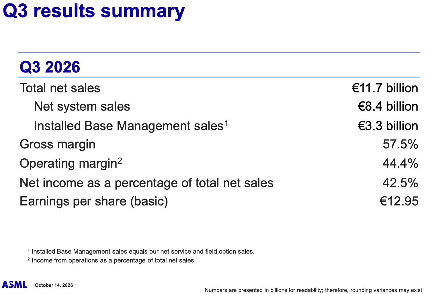
ASML this week reported record quarterly revenue of $13.06 billion (€11.66 billion) and profitability of nearly $5.79 billion (€5 billion) as demand for advanced semiconductor manufacturing equipment continues to accelerate and investments in AI infrastructure continue to increase. The company now expects demand for its lithography systems to exceed its production capacity in 2027 and 2028, despite plans to increase output substantially. Some clients are already interested in placing orders for equipment as far ahead as 2030, which makes ASML consider further capacity expansions beyond its previously announced intentions.
Record financial results
ASML reported third-quarter 2026 revenue of $13.06 billion USD (€11.66 billion), up 55% year-over-year and 25% sequentially. The company's gross margin reached a record 57.5%, up from 51.6% a year earlier, while operating income rose to $5.79 billion (€5.17 billion). Net income reached $5.56 billion USD (€4.96 billion) , although this figure includes approximately $570 million (€510 million) from the re-evaluation of the company's investment in Mistral AI.
(Image credit: ASML)
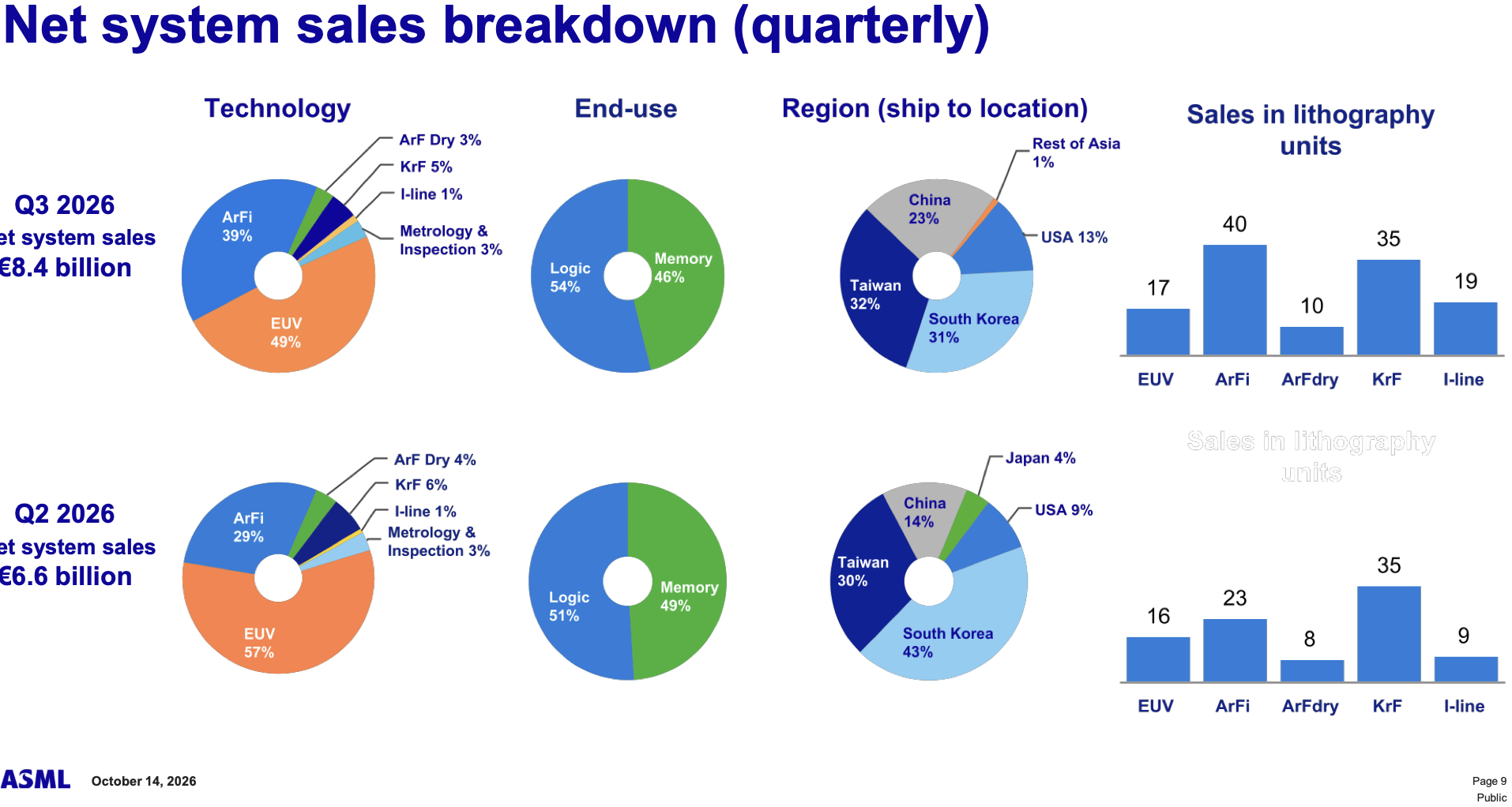
During the quarter, ASML sold 121 lithography systems, including 113 new and eight refurbished machines, up from 91 systems in Q2 2026. The company generated $4.59 billion USD (€4.1 billion) from 17 EUV lithography systems and $4.82 billion USD (€4.3 billion) from 85 DUV (including 45 ArFi scanners) and 19 i-line litho tools. In addition, ASML recognized revenue from one High-NA EUV system in Q2. Of total equipment revenue, 54% came from logic chipmakers and 46% from memory manufacturers.
(Image credit: ASML)
Taiwan accounted for 32% of ASML's equipment sales in Q3 2026, followed closely by South Korea at 31%. China represented another 23%, while the United States accounted for 13% and the rest of Asia contributed just 1%. Combined, Taiwan and South Korea generated 63% of ASML's equipment revenue, which reflects substantial investments in advanced logic and memory manufacturing capacity that by far exceed those in the U.S. and Japan.
(Image credit: ASML)
ASML’s Installed Base Management business generated $3.68 billion (€3.29 billion), approximately $450 million (€400 million) above guidance, largely due to strong demand for productivity upgrades (more on this later), which contributed to the company’s record profitability.
For the fourth quarter, ASML expects revenue of $15.9 billion to $17.0 billion (€14.2 billion to €15.2 billion) and gross margin of approximately 57%. Full-year revenue should reach $49.3 billion to $50.4 billion (€44 billion to €45 billion), up approximately 36% YoY. The company projects EUV revenue should increase by more than 45% year-over-year, while memory-related equipment sales are expected to rise by approximately 75%, which indicates growing demand from DRAM producers.
Demand for litho tools spans to 2030
One of the biggest learnings from these results and accompanying statements is that semiconductor manufacturers are increasingly interested in securing lithography equipment years before they actually need it. According to ASML CEO Christophe Fouquet, customers expect demand for its products to exceed available supply through at least 2028, which encourages them to accelerate construction of new fabs as well as expand their existing capacity.
"Our leading-edge high-volume customers are sharing very good visibility as a result of the increasing number of long-term commitments they are securing with their customers," Fouquet said during the company's conference call with analysts and investors. "This extended visibility has led them to conclude that demand for their products will outpace supply through at least 2028. As a result, customers are accelerating capacity build-out plans and preparing for further expansion beyond 2028 in order to better meet the anticipated level of demand."
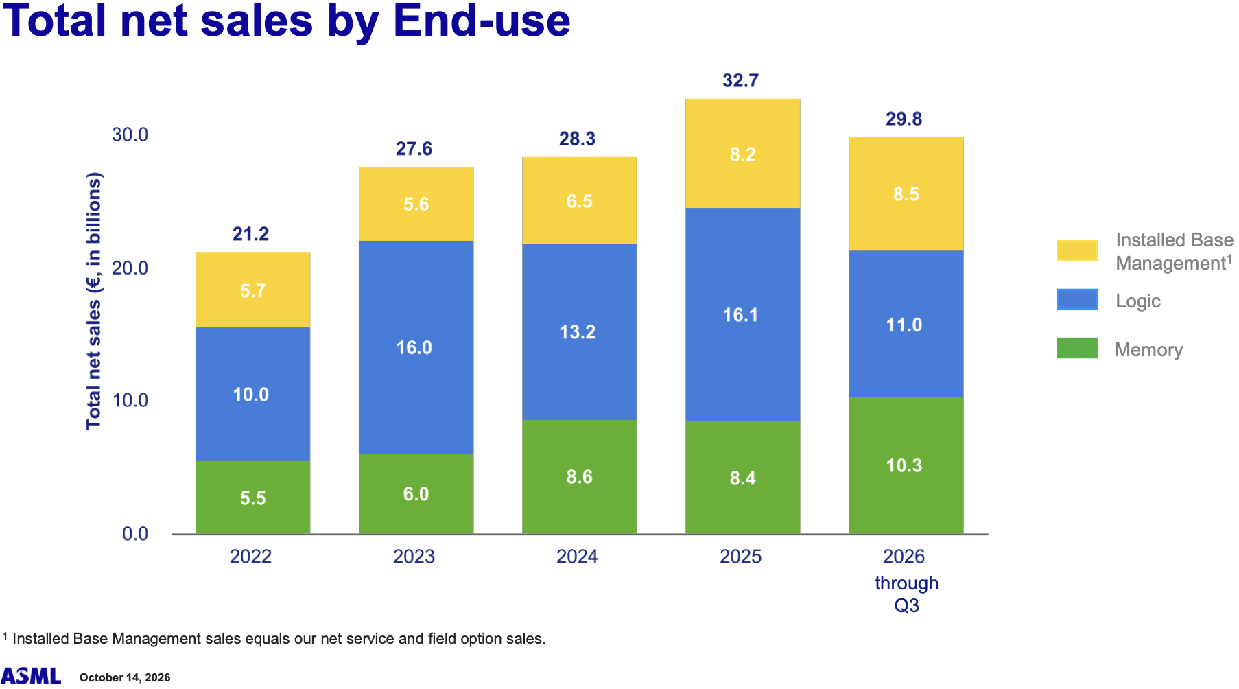
(Image credit: ASML)
ASML is already receiving orders that are to be delivered in 2028, while some customers have expressed interest in equipment for 2029 and even 2030.
"As customers shift focus to their needs beyond 2027, our order momentum continues to build," Fouquet added. "We are increasingly receiving orders for 2028, and customers are also expressing interest in placing orders for 2029 and even 2030."
To address this demand, ASML plans to manufacture approximately 65 Low-NA EUV systems in 2026, up from 44 scanners shipped in 2025. Production of immersion DUV systems should remain approximately at last year's level, even though proveiously the company expected shipments of DUV tools to decline.
The company previously announced plans to increase production capacity for both Low-NA EUV and immersion DUV systems by 30% in 2027, followed by another potential 30% increase in 2028. Based on its 2026 EUV production target, this implies capacity for approximately 85 Low-NA EUV systems in 2027 and roughly 110 in 2028, assuming both increases materialize.
However, ASML now believes even this level of output will be insufficient and is investigating ways to expand its 2028 capacity beyond the previously planned 30% increase. However, the company has not disclosed revised production targets.
"Looking further ahead, we shared our intent last quarter to increase our capacity in 2027 by 30% for both Low NA EUV and DUV immersion systems, as well as to investigate adding a further 30% in 2028," explained Roger Dassen, Chief Financial Officer at ASML. "However, given the dynamics of this quarter, we now anticipate that our current planned levels of output in 2027 and 2028 will not fully meet the demand of our customers."
High-NA EUV adoption
Meanwhile, High-NA EUV adoption is progressing. Intel has already exposed more than one million wafers using High-NA systems and plans to start using High-NA EUV with its 14A process technology in 2028. Samsung plans to introduce High-NA EUV into high-volume manufacturing (HVM) in 2028 for DRAM and for logic later, while TSMC plans to use High-NA EUV scanners by 2030 – 2031. ASML says availability across its installed High-NA fleet is approaching 90%, which suggests that the tools are becoming mature enough for HVM deployment.
(Image credit: ASML)
Interestingly, Samsung's planned 2028 introduction may create additional demand for High-NA equipment from memory manufacturers, as they will need to compete against their larger rival. However, ASML has not disclosed specific shipment targets for these tools.
New tools, more capacity
ASML also intends to increase semiconductor production capacity by introducing more productive lithography systems. Its upcoming Twinscan NXE:3800F, scheduled for introduction in early 2027, will process up to 260 wafers per hour, compared with 230 wafers per hour for the existing NXE:3800E. While this represents 'only' approximately 13% higher throughput, this translates to 21,600 extra EUV exposures per month without corresponding increases in cleanroom space. Three such tools per fab enable 90 additional EUV exposures per hour, 2,160 per day, or 64,800 per month. The company also plans to introduce a new critical-layer immersion DUV system capable of processing 330 wafers per hour.
(Image credit: ASML)
Keep in mind that the actual fab capacity improvements depend on the number of lithography exposures required per wafer on a particular node, as well as the capabilities of other manufacturing equipment.
ASMLASML
Another important element of ASML's strategy is its growing portfolio of productivity upgrade packages for existing EUV and DUV systems. Such upgrades enable chipmakers to increase wafer throughput without purchasing additional scanners, which can provide additional capacity considerably faster than procuring new tools or constructing new fabs.
Value-based pricing is a go
One of the controversial things that ASML discussed back in early Q2 was its value-based pricing, which many thought was a blanket price hike. This is not and CFO Roger Dassen this week confirmed that negotiations with major customers have been completed, although the financial benefits for ASML will not become visible immediately.
(Image credit: ASML)
The company expects the first effects of higher pricing to appear during 2027, with the full impact becoming apparent in 2028 and beyond, which essentially means that the company is not setting new prices on its backlog, but generally setting new prices on new tools.
"We completed those conversations," said Dassen. "So that has been done with the key customers. The effect of that is not really visible in 2026. It will start to become visible partly in the course of 2027. The full impact of that you will start to see in 2028 and beyond."
This strategy could further improve ASML's already substantial gross margins, particularly as customers have no alternatives for advanced lithography equipment.
China remains important
Despite export restrictions that prevent Chinese chipmakers from acquiring EUV scanners and advanced DUV systems, China remains a substantial market for ASML. The company expects China to account for approximately 20% of its total revenue in 2026, which implies annual sales of roughly €8.8 billion to €9 billion based on current guidance.
(Image credit: ASML)
Although China's share of ASML's business has declined from its levels in 2023 - 2025, the country's semiconductor manufacturers continue to invest in mature node capacity and equipment that remains available under existing export regulations. Meanwhile, it is impossible to predict what is going to happen if the U.S. lawmakers approve the MATCH Act.
Yet, ASML management emphasizes that its key growth opportunities lie with advanced logic and memory manufacturers, which are accelerating their investment in advanced lithography tools, including sophisticated DUV systems, Low-NA EUV machines, and High-NA EUV scanners.
The future of ASML
Thanks to gaining momentum in AI infrastructure investments, ASML reported record quarterly revenue of $13.06 billion (€11.7 billion) as demand for advanced lithography equipment continued to accelerate. The company expects demand to persist for years as its customers are interested in placing orders for tools to be delivered as far ahead as 2030. To meet growing demand, the company plans to expand production capacity beyond its previous targets for 2028. ASML also intends to introduce new EUV and DUV systems with higher productivity, offer productivity upgrades, and raise equipment prices to capitalize on unprecedented demand.
ASML has said that the unprecedented spending and investment brought about by the artificial intelligence (AI) boom is not slowing down at all, as customers are already lining up to place orders for its advanced chipmaking tools for 2029 and 2030, according to a Reuters report citing ASML's Q3 2026 earnings published today, October 14. ASML CEO Christophe Fouquet said that the company would struggle to meet the demand despite plans announced in July to raise capacity by 30% in 2027 and another 30% in 2028. The company also confirmed on Wednesday that it will raise prices starting in 2027, with the full effect showing in 2028.
The Dutch company's comments follow its Q3 2026 earnings report, which detailed a net profit of €4.96 billion on net sales of €11.7 billion. It projects Q4 sales of €14.2 billion to €15.2 billion ($15.9 billion to $17 billion), boosting its full-year sales projections from at least €43 billion to €44-45 billion. ASML's shares rose 2% on Wednesday, up almost 70% so far this year, with its €586 billion market valuation making it Europe's largest firm by market cap.
According to Reuters, there had been concerns that the AI investment boom was losing steam. However, positive projections from the largest manufacturer of the tools for making AI chips and advanced semiconductors signal that chipmakers will keep expanding, sustaining demand across the AI industry well into the foreseeable future. "There were concerns that the AI trade was running out of steam," Gordon Kerr, European macro strategist at KBRA, said. "Demand for chips remains strong, and infrastructure spending is likely to continue well into 2027."
ASML's order book reflects a wave of spending across the AI industry. As of April this year, Google, Amazon, Microsoft, and Meta reportedly collectively planned to spend $725 billion on capex in 2026, up 77% from last year's record $410 billion. Since then, Alphabet has raised its 2026 capex guidance from $180–190 billion to $195–205 billion, Amazon from $200 billion to $220 billion, and Meta has raised the floor of its range from $125 billion to $130 billion, keeping its $145 billion ceiling. Some of the spending reflects rising chip prices, with Microsoft CFO Amy Hood attributing $25 billion of the company's record capex budget to higher prices for memory chips and other components. Still, analysts such as Gartner expect global AI spending to rise 49.5% in 2026 to $2.7 trillion and another 36.2% in 2027.
C.C. Wei, chief executive and chairman of TSMC, confirmed on Thursday that the company is considering expansion of its American production capacity beyond Arizona and Texas is one of the options it is evaluating. The head of the world's largest contract chipmaker also confirmed negotiations with Elon Musk regarding usage of Terafab, but stressed that to be a part of it, the fab must be managed by TSMC, which automatically excludes burgers and cigars in the cleanroom.
"We expanded our capacity consideration to see outside Arizona, whether we can get another chance to expand our capacity," said C.C. Wei during the company's earnings call with financial analysts and investors. "Texas is one [of our options]. We sent the teams to Texas to do all the evaluation. We also talked to one of our customers, who is trying to build a fab, Terafab, let me be more specific."
"We are discussing with them to see whether we can be utilizing that actual capacity also," Wei added. "So, we are still in discussion. If we have any solid conclusion, we will share with you."
The information about negotiations between Elon Musk's Terafab and TSMC immediately triggered chatter that the parties are set to adopt TSMC's typical business model it uses for ESMC and JASM facilities under which it operates fabs co-owned with other investors. However, Musk then said that Terafab's facility would be operated by Terafab and TSMC could only sub-lease part of its cleanroom. Now, C.C. Wei said that if TSMC joins the project, it will insist on operating the fab.
"We are still in discussion," Wei replied when asked whether TSMC is not becoming a part of the Terafab project. "Let me say that. […] Either way, it will be possible, but the fab has to be run by TSMC."
The key question now is whether Musk and TSMC can agree on an arrangement that satisfies both parties. Musk wants Terafab to retain control of its manufacturing complex, whereas TSMC insists on operating any fab it uses. One potential compromise would be for Terafab to own the facility and lease a portion of it to TSMC, which would independently operate its production lines. Such an arrangement would allow Musk to retain ownership of the whole complex while giving TSMC control over select manufacturing lines. However, if Terafab itself uses Intel's 14A process technology at the facility, TSMC's presence there will be extremely complicated, if possible at all. In any case, so far the parties have not come to any agreement.
TSMC on Thursday reported revenue of $46.72 billion for the third quarter of 2026, up 41.2% year-over-year and 16.2% sequentially. The foundry's net income reached approximately $23.9 billion, an increase of 68.7% from the same quarter a year earlier, driven by elevated demand for chips used by AI infrastructure. The company's gross margin was 66.4%, which is below gross margins reported by DRAM makers, but still a historic record.
For the fourth quarter of 2026, TSMC expects revenue between $52.3 billion and $54.3 billion, which represents approximately 14% sequential growth at the midpoint. The company projects gross margin between 65% and 67%, up both sequentially and YoY.
Geopolitics and sanctions have mostly cut off the Russian public from Western hardware — at least officially. In recent ages, the country's homegrown chip designs are Arm, RISC-V, and Elbrus architectures. A handful of interesting designs were on display at the Microelectronics 26 (ME26) forum in Sochi, using retro gaming as a demonstration point. A couple of years back, the government even issued an order to create a high-end gaming console, albeit with relatively little success. The result of that initiative didn't appear to be on display at the event.
На выставке МЭ26 в Сочи показывали сразу несколько игровых применений русских процессоровБайкал: консоль и визитка на Ушке BE-U1000Элвис: полноценная приставка на Гиперком У (бывш. СКИФ)МЦСТ: «игровые» ПК на ЭльбрусахНе серьёзно, но занимательно#riscv #innoru #pureru https://t.co/QGlRTMnvLROctober 11, 2026
The report comes from Dmitrii Kuznetsov, a RISC-V and Rust enthusiast who displayed photos from the event. The first units on display use Baikal Electronics' BE-U1000 microcontroller. According to our digging, the chip packs a CPU with three CloudBear cores (32-bit RISC-V) — two BR-350s clocked at 200 MHz, along with a BM-310 at 100 MHz.
Given the microcontroller nature, embedded resources are intentionally sparse, with 256 KB of flash and 192 KB of SRAM — though there's support for external flash. A host of I/O interfaces, including USB 2.0, I2C, I2S, UARTs, and 48 GPIO lines, round out the 10x10 mm QFN-88 package. These parts are seemingly aimed at robotics, automation, IoT, sensors, and similar applications.
There was a business card-sized controller-and-console on display with a BE-U1000 chip, along with an "Ushka" console styled like the original NES (with matching controllers). The game on display appears to be Chip 'n Dale: Rescue Rangers.
Next up, there's the Elvis Hypercom-U, a SoC packing four Arm Cortex-A53 CPU cores at up to 1.2 GHz, dual ELcore-50 DSPs, a PowerVR GE8300 GPU, and dedicated video, image, and navigation processing blocks. The main silicon can be paired with up to 8 GB of LPDDR4, and supports USB 3.0, Gigabit Ethernet, Wi-Fi, and Bluetooth connectivity, and HDMI output.
This product is apparently aimed at multimedia, navigation, SBCs, and smart cameras. At the show, a board with the Hypercom-U was shown playing the original Super Mario as a demonstration.
Finally, there were MCST's Elbrus-based PCs, though the tweeter offered few details on which were on display. For context, Elbrus is a Russian-developed chip architecture, often poised as the basis for high-end desktop and server applications.
Our best guess is that the machines at the forum were based on the leading-edge Elbrus-16S chip with 16 cores at up to 2 GHz and up to 8 channels of DDR4-3200 RAM. The chip is manufactured on a 16 nm process and comprises 12 billion transistors. There are dual-processor server prototypes with up to 2TB of RAM using this design.
The other chip likely being demoed is the Elbrus-2S3, a chip targeted at mini-PCs and laptops. We've covered the Rostec MP21 previously, a Raspberry Pi-like machine with 8GB of RAM and SSDs up to 480GB. The 16-nm SoC is fairly decent, clocked at up to 2 GHz and capable of 196 GFLOPS. There's support for DDR4-3200 and PCIe 3.0, but power consumption can be fairly nasty, as the MP21 board can chew around 40W.
Two workers have been confirmed dead and another seriously injured after an explosion at Intel’s Kiryat Gat plant in southern Israel on Wednesday, The Times of Israelreports. Police suspect a gas cylinder malfunction caused the explosion, and Israel’s Fire and Rescue Services said the fire involved nitrogen trifluoride (NF3), a toxic gas mainly used to clean the process chambers of chipmaking tools. So far, Intel hasn’t made any statements about the victims or about any potential production impacts at the site.
The site houses Fab 28, which, per Intel, makes “processors, 5G, and AI products” on Intel 7, formerly 10nm Enhanced SuperFin. Intel 7 products include 13th and 14th Gen Core “Raptor Lake,” 5th Gen Xeon “Emerald Rapids,” and the I/O die of Xeon 6 “Granite Rapids,” although these are not explicitly linked to the site. Fab 38, adjacent to Intel’s existing Kiryat Gat fabs, was announced in December 2023 with a $3.25 billion Israeli grant but has been paused since mid-2024. Intel reportedly considered closing Fab 28 in July 2025, but no closure decision has been announced.
The Kiryat Gat police commander at the scene laid out the sequence: a blast occurred during a material transfer into the factory’s tanks after one truck had disconnected and another connected. At least eight Fire and Rescue Services teams, including hazmat, searched for trapped people, contained the fire, and monitored the hazardous substance.
“At this moment, I cannot point to any suspicion of criminal activity or negligence,” the commander added. Magen David Adom, Israel’s national emergency medical service, said two of the injured underwent resuscitation efforts and all three suffered severe burns. Ultimately, one of the injured was pronounced dead, a second later died of their wounds, and one remains hospitalized in serious condition inside the ICU, based on a statement from Soroka Medical Center in Beersheba.
The gas, although hazardous if inhaled, is not flammable. It’s not clear if the trucks were delivering NF3 or if it was directly involved in causing the explosion. Once the fire was put out, crews kept cooling the scene to prevent a secondary incident, and the commander said things appeared to be under control, with no sign so far of further leaks and no need to evacuate residents or factory workers. Kiryat Gat Mayor Kfir Suissa told residents to stay away while crews worked and added, “There is no danger to the public.”
At the time, there was no word on possible production delays, but these would be problematic as Intel 7 capacity was already tight. Last year the company’s CFO said that Intel 7 and Intel 10 constraints had limited its ability to meet demand, with shortages expected into 2026 with server wafers getting priority. Intel reports third-quarter results on Oct. 29 and will hold a call to discuss them, although the company has not mentioned whether it will address the explosion.
 登录