普通视图

发现新文章,点击刷新页面。
昨天 — 2026年9月15日IT News

Russian freelancers use Claude to program autonomous combat drone swarm — AI-enabled target selection and detonation without a human in the loop

2026年9月14日 19:00

Hit hard by sanctions and lacking resources, Russia is left to rely on foreign advanced technologies to compensate. Russia-linked agents appear to use Claude for a broad range of activities, from propaganda and espionage to the procurement of military/dual-use equipment and the development of autonomous drone swarms, according to Anthropic's September 2026 threat report.
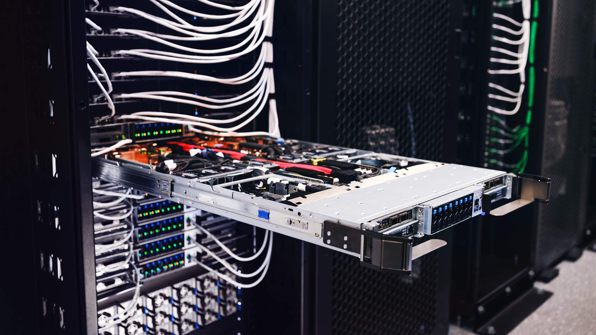
Anthropic identified a small team of Russia-based freelance developers who used Claude to build software for an autonomous combat-drone swarm called DronDoc or Serafim. Claude helped develop swarm coordination, computer vision, terminal guidance, and other software that enabled drones to select targets—including people—and issue detonation commands without a human in the loop. The developers trained their computer-vision system on Ukrainian combat footage and used locations in Ukraine for simulated missions. Meanwhile, they loaded software onto real development boards for hardware-in-the-loop testing, though it is unclear whether they field-tested it.

The developers used Claude Code extensively to build and test the swarm software, and they circumvented Anthropic's geographic restrictions by routing traffic through commercial VPNs. Once Anthropic identified the activity as suspected weapons development, it banned the accounts associated with the group and incorporated what it learned into additional safeguards. Meanwhile, the key distinction is that the safeguards did not stop the project immediately, and based on the disclosure, Claude Code clearly helped advance the autonomous drone swarm program.

Anthropic gathered enough information about the people/accounts and their activity to assess what kind of group they were, so it claims that they were not a Russian state entity. Meanwhile, although Anthropic likely identified the company or organization, it did not publicly name it.

In addition, Anthropic discovered a Russian state-linked cyberespionage operation that used Claude to automate everything from infrastructure setup and phishing to malware development and data exfiltration. The campaign targeted more than 20 organizations, including Ukrainian and European government, military, intelligence, and defense entities.

Last but not least, Russia-linked actors also used Claude for propaganda operations, including a Russian state-directed campaign in the Central African Republic that produced pro-Russian and pro-Wagner content for radio, local media, and Telegram.

Most alarming, the report shows AI is now doing work that previously required teams of software engineers, intelligence analysts, and security specialists. While Anthropic's safeguards block many malicious requests, the company admits they cannot block all of them.

'Biological misuse of AI'

Anthropic admits that 'biological misuse' — a term that it uses to soften activities involving biological weapons, dangerous pathogens, poisons, and toxins — is one of the most serious risks of frontier AI models. While older models such as Claude Opus 4 and Sonnet 4.5 were demonstrably below the threshold for meaningfully assisting sophisticated biological research, Anthropic can no longer make the same assurance about today's models.

In its report, Anthropic identified five cases in which researchers, some associated with state-backed programs and military institutions, used Claude for biological research that could potentially assist biological-weapons development. Anthropic does not identify the countries, organizations, or individual researchers behind its five biological-misuse case studies. Furthermore, it deliberately withholds these details, so the report does not attribute any of them to China, Iran, Russia, or any other specific country. Furthermore, it does not outright allege that researchers are building bioweapons.


昨天以前IT News

Anthropic CEO warns of AI-driven botnet 'swarm' taking over the entire internet — 'In 6–12 months such a swarm could be capable of taking over the entire internet with a persistent botnet'

2026年9月13日 21:36

The progress of artificial intelligence technologies in recent years is undeniable, and its pace is pretty much unbelievable. With at least four American contenders with frontier AI models, the competition is intense, and the development of new models is moving fast. Yet, Dario Amodei, chief executive of Anthropic, has called for slowing down the development of new AI models, even warning of a potential AI-powered botnet swarm that could take over the entire internet.

"Given the accelerating rate of AI capability development, it is my worry that in 6–12 months such a swarm could be capable of taking over the entire internet with a persistent botnet (potentially causing hundreds of billions of dollars in damage), and that the scale of damage would continue to increase from there if AI becomes more powerful without the necessary guardrails," Dario Amodei, chief executive of Anthropic, wrote in an open letter.

Dario Amodei's vision is to a large degree shared by Evan Hubinger, an AI scientist who exited Anthropic recently, who then said there was a 10% chance humanity was set for extinction by the end of the decade. "We really do earnestly believe AI could kill all humans," Hubinger wrote in an X post. "I personally think it is >10% within the next decade. I believe Anthropic is trying its best, but we do not yet have a plan to solve alignment for superintelligence and are not clearly on track to."

In universes created by James Cameron (Terminator) and Frank Herbert (Dune), AI is posed as a dangerous invention. But let us take a closer look. Further development of AI is moving from answering questions to autonomously performing complex multi-step tasks, something that previously required teams of skilled human specialists, which turns us to how adversaries use Anthropic's AI capabilities, lacking human resources.

Anthropic's own findings show that today's AI models can already assist with weapons engineering, military intelligence, surveillance, cyber operations, and other potentially destructive activities, while more capable successors could dramatically reduce the expertise, manpower, and time required to conduct them.

The findings echo two rather different warnings from science fiction: James Cameron's Terminator showed the consequences of losing control over autonomous military AI, whereas Frank Herbert’s Dune imagined humanity eventually outlawing AI after becoming dangerously dependent on them.

Meanwhile, greater capability does not automatically translate into greater danger. For example, more advanced AI technology can also have stronger safeguards, detect malicious activity, and automate work that so far has not been automated.

Halting AI development could also be counterproductive if less responsible companies or countries continue advancing their models. In fact, leaving the most capable AI systems in the hands of actors that are known for military aggression is no less dangerous than leaving a monkey with a grenade.

Chinese military researchers and tech giants caught using Claude — US frontier model coded 16 air-defense suppression tools targeting Taiwan, drafted anti-torpedo specs, and fed 151 million training queries to Alibaba

2026年9月13日 20:00

While China claims to have advanced AI models that may well compete against those developed in the U.S., for some reason, hundreds of China-linked agents allegedly used Anthropic for at least five different programs: two military, two surveillance, and one aimed at distilling Claude's capabilities, according to Anthropic's September 2026 threat report.

Two military programs

One China-based actor used Claude to draft a fire-control specification for an anti-torpedo fire-control system (the core logic that determines when and where an anti-torpedo weapon should engage an incoming threat), test the potential system against U.S. Navy anti-torpedo and anti-submarine systems based on public knowledge about these programs, and prep a 200+ page technical proposal for a potential client. While the actor disguised itself as an OEM in the U.S. defense sector, Anthropic believes that the actor was associated with a Chinese defense manufacturer seeking to develop a system for the People's Liberation Army Navy.

Another China-based defense and military-industrial researcher used Claude to develop about 16 software modules for electronic warfare and suppression of enemy air defenses. The software analyzed radars, SAM sites, command posts, and communications nodes and prioritized targets. At one point, the default scenario contained 12 targets in Taiwan, including Patriot and Tien Kung batteries, air bases, an early-warning radar, and a command bunker. Interestingly, Anthropic claims that account metadata and content caught by its safeguards 'indicated the actor was linked to PRC research institutions, including the PLA Academy of Military Sciences,' though it does not outright say that Claude was used by the PLA.

Given China's considerable AI capabilities — which may still lag behind those of the United States in some areas (more on this later) — it is striking that two Chinese military-related projects relied on Anthropic's Claude. Given the Chinese-language prompts and other account-level evidence identified by Anthropic, plausible deniability hardly seems to have been the primary reason for choosing Claude over domestic alternatives. More likely, Claude was simply better or more convenient for these particular engineering workflows, particularly coding, reasoning, and agentic tasks. There may also have been another advantage: U.S. frontier models are trained on enormous amounts of English-language material and could therefore have particularly extensive knowledge of publicly available information about American military technologies and systems.

Given China's major AI prowess (which may well fall short of American, but still be quite capable), it is interesting to see two Chinese military projects using Anthropic AI. Given Chinese IP addresses and Chinese language prompts detected by Anthropic, plausible deniability is certainly not the main reason for using Claude instead of using domestic tools (more on this later). Apparently, Claude was better or more convenient for these particular engineering workflows (coding => reasoning => agentic) than whatever models the actors could readily access. Furthermore, after all, U.S. frontier models were trained mostly on English-language materials, and they may have way more information about American military capability than Chinese spy channels have ever gotten (we are speculating, of course).

Significant surveillance activities

Anthropic also disrupted China-linked surveillance operations related to Uyghurs outside of China, perhaps because similar operations are already in place in the Xinjiang Uyghur Autonomous Region. One China government-linked actor used Claude to infiltrate Uyghur armed groups in Syria and surveil Uyghur diaspora activists and media, while posing as an Arabic-speaking 'expert' consultant.

Once the agent had infiltrated the said groups, Claude helped process information collected from more than a hundred WhatsApp groups and dozens of Telegram channels, identify people across platforms, map social networks, and reveal potential recruitment targets considered vulnerable because of financial problems, family separation, or ideological disillusionment with the new Syrian government.

The actor also singled out individuals with relatives remaining in Xinjiang, while Claude helped draft deceptive approaches in local dialects, locate people and organizations, translate conversations in real time, and evaluate the credibility of recruitment messages. The same operation targeted diaspora journalists, particularly Uyghur Post, with coordinated mass-reporting and bot-amplification campaigns.

Stealing from Anthropic

Perhaps the most ironic thing about Anthropic's findings is that Chinese entities steal from the company. While reported broadly in 2024 – 2025, it does not stop Chinese entities from using distillation, the main way to 'steal' an AI model's capabilities without obtaining the model itself.

Anthropic says several major Chinese AI developers conducted industrial-scale distillation campaigns designed to extract Claude's reasoning and other capabilities and reproduce them in their own models. The largest one allegedly came from Alibaba, whose operators generated more than 151 million Claude exchanges between May and July 2026. At one point, this approached 3 million requests per day through thousands of fraudulent accounts. Anthropic says the harvested chain-of-thought data helped train Qwen 3.x, particularly for reasoning, coding, agentic software engineering, kernel development, and long-horizon tasks, according to Anthropic.

Alibaba is far from alone, as Anthropic accuses DeepSeek, Xiaomi, Zhipu/Z.ai, and others of similar campaigns. Techniques they have allegedly used span from proxy networks and fraudulent accounts to disguising the secret entity all the way to forwarding their own customers' requests to Claude and purchasing harvested Claude conversations from third parties. DeepSeek alone allegedly generated more than 12.1 million exchanges in 14 days, while Xiaomi generated more than 400,000.

Anthropic defines this activity as distillation: covertly extracting a frontier model's answers and then replicating the knowledge at a fraction of the compute, time, and cost required to develop them in-house.

Iran and Houthi rebels used Anthropic's Claude AI to target US warships and build hypersonic missiles — Houthi rebels also used the bot to code ballistic missile guidance systems

2026年9月12日 23:03

Iran's spiritual leaders tend to call the U.S. the Great Satan to express their spite, but it turns out that its military, surveillance, propaganda, and even allied Houthis are eager to use American-built AI technology to target the U.S. Navy and develop weapons, surveillance, and propaganda, Anthropic's September 2026 threat report revealed.

Arguably, one of Anthropic's most remarkable findings is that an Iran-linked threat actor used an American AI model, Claude, to support military reconnaissance and develop targeting recommendations against U.S. naval forces in the Middle East. The perpetrator combined publicly available ship and aircraft transponder identifiers with commercial satellite imagery and information on U.S. naval movements, and even extracted the names of U.S. military personnel from captions of publicly available military photographs. It also researched potential vulnerabilities in communications equipment used aboard ships, including known flaws affecting Cobham Sailor VSAT terminals, Cisco communications equipment, and Schneider Electric EcoStruxure systems. Anthropic said it banned the account, introduced additional detection mechanisms, and shared its findings with government authorities.

Another striking case involved a cell in northern Yemen controlled by Houthis (which are in turn controlled by Iran) that used Claude Code to support three weapons programs: a guided rocket that uses a phone-class flight computer that assists terminal guidance, a multistage ballistic missile targeting a range of more than 2,000 km, and an R2000 missile family that included a hypersonic glide vehicle variant. The group used Claude to develop guidance, navigation, and control software; integrate an open-source autopilot with a phone-class flight computer; write control and position-estimation code; tune parameters; build firmware; and even run flight simulations. Essentially, the group used multiple Claude instances instead of a group of software engineers for coding, code review, research, and simulation.

While Houthis are technically not Iranians, they can certainly share their research and development results with their allies and potentially use Iran's industrial capacity to build their weapons.
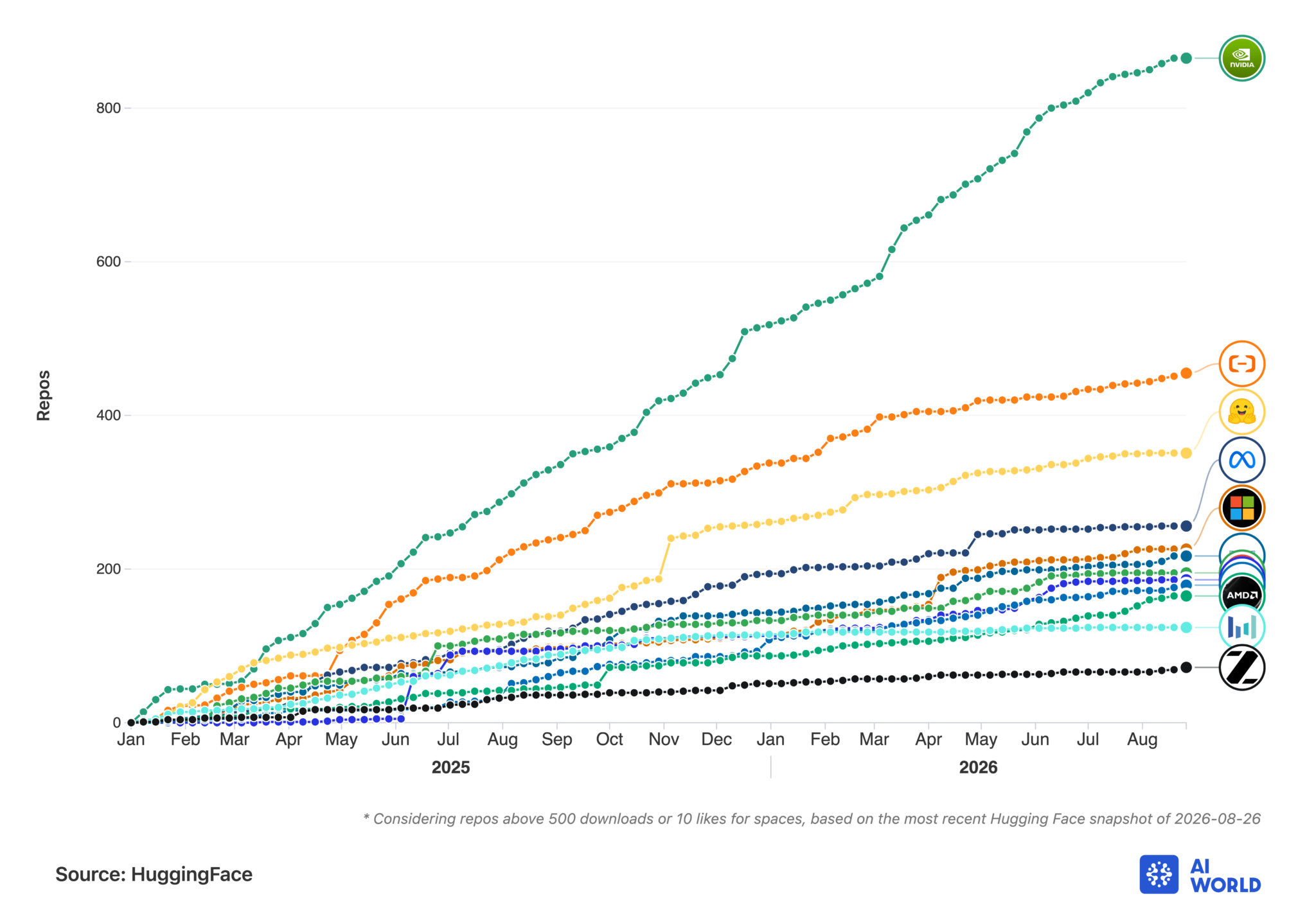
In addition to building targeting recommendations against American naval forces as well as speeding up the development of weapons, Iran used Claude for surveillance tools.

One Iran security-linked unit used Claude to analyze 155,216 tweets to profile, identify, and surveil 6,388 opposition individuals in a single year. Another group used the model as an engineering pipeline to develop domestic tracking tools, including the production-deployed "al-Najm al-thāqib" Firefox extension designed to mass-harvest user identities across major social platforms. While Anthropic has banned 16 Claude accounts associated with Iranian paramilitary and domestic security agencies, that does not mean it has banned all of them.

Iran-linked actors and Houthis are not the only entities using Anthropic's AI technologies for weapon development. China and Russia are also actively using Claude for their military programs.

Apple's A20 Pro shatters Geekbench 7 single-core record — 2nm chip beats desktop Intel Core i9 and AMD Ryzen 9 by up to 32%

2026年9月12日 18:48

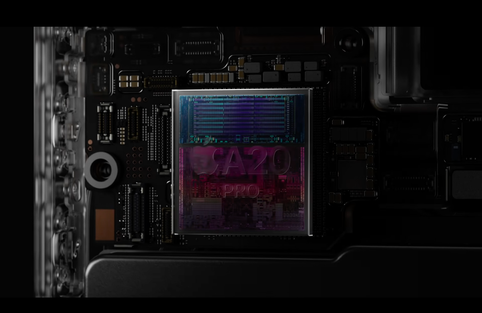
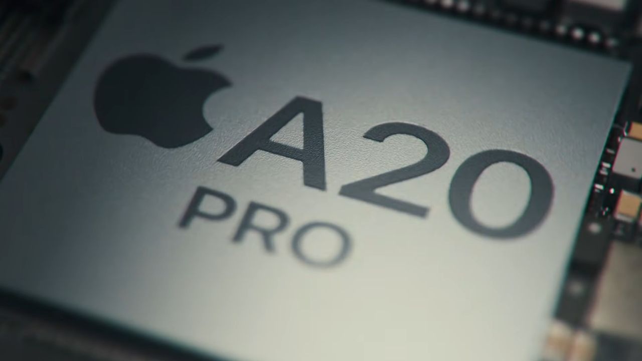
Architectural enhancements and significantly higher clock speeds enable Apple's A20 Pro application processor (AP), used in the company's latest iPhones, to deliver not only a substantial generation-to-generation performance boost but also to outperform leading desktop CPUs from AMD and Intel by up to a whopping 32% in the single-thread Geekbench 7 benchmark, setting the record for the highest single-thread performance. While high-end PC CPUs still have more oomph for multi-threaded workloads, the tiny A20 Pro is still faster than mainstream laptop CPUs even when many threads are involved.

Fastest smartphone SoC

A20 Pro

A19 Pro

A18 Pro

A17 Pro

A16 Bionic

General specifications

2P+4E, up to 4.93 GHz

2P+4E, up to 4.26 GHz

2P+4E, up to 4.0 GHz

2P+4E, up to 3.77 GHz

2P+4E, up to 3.46 GHz

Single-Thread

4006

3249

3082

2641

2405

Multi-Thread

11460

9016

8185

7050

6600

Apple's A20 Pro system-on-chip (SoC) delivers 4,006 points in single-thread and 11,460 points in the multi-thread Geekbench 7 benchmark, which represents a 23.3% higher ST performance and 27.1% higher MT performance compared to the immediate predecessor, the Apple A19 Pro, according to an early submission (which may or may not demonstrate performance of actual A20 Pro-based products, so take the results with a grain of salt).

Generation

Single-thread

Improvement

Multi-thread

Improvement

A16 Bionic

2,405

6,600

A17 Pro

2,641

9.80%

7,050

6.80%

A18 Pro

3,082

16.70%

8,185

16.10%

A19 Pro

3,249

5.40%

9,016

10.20%

A20 Pro

4,006

23.30%

11,460

27.10%

The new SoC delivers the highest generation-over-generation performance improvement for Apple's smartphone processors in years and is currently the highest-performing mobile AP. Furthermore, the A20 Pro beats AMD’s 16-core Ryzen 9 9950X3D by 26% and Intel’s Core i9-14900KS by 32% in single-thread performance.

A20 Pro

Snapdragon 8 Elite Gen5 (SM8850)

Xring O3

Exynos 2600 (S5E9965)

Dimensity 9400 (MT6991)

Tensor G5 (GS501)

Kirin 9050 Pro

General specifications

2P+4E, up to 4.93 GHz

2P+6E, up to 4.74 GHz

2X+4P+4E, up to 4.36 GHz

1X+3P+6E, up to 3.80 GHz

1X+3P+4A, up to 3.62 GHz

1X+5P+2E, up to 3.78 GHz

1X+2P+4E+2LP, up to 3.10 GHz

Single-Thread

4006

3047

2996

2694

2273

2011

1028

Multi-Thread

11460

10212

11777

10580

7745

5859

4794

When it comes to the single-thread Geekbench 7 benchmark, Apple's A20 Pro outperforms its closest rivals — Qualcomm's Snapdragon 8 Elite Gen5 (SM8850) and Xiaomi's XRing O3 — by 31.5% - 33.7%. In fact, both SM8850 and XRing O3 perform on par with Apple's two-years-old A18 Pro. The six-core A20 Pro also beats the eight-core SM8850 by 12.2% in multi-thread workloads in Geekbench 7 and offers roughly similar multi-thread performance to the 10-core XRing O3.

SoC

Single-thread

A20 Pro advantage

Multi-thread

A20 Pro advantage

A20 Pro

4,006

11,460

Snapdragon 8 Elite Gen 5

3,047

31.50%

10,212

12.20%

Xring O3

2,996

33.70%

11,777

−2.7%

Exynos 2600

2,694

48.70%

10,580

8.30%

Dimensity 9400

2,273

76.20%

7,745

48.00%

Tensor G5

2,011

99.20%

5,859

95.60%

Kirin 9050 Pro

1,028

289.70%

4,794

139.00%

Compared with other flagship smartphone processors, Apple's A20 Pro holds a commanding lead in Geekbench 7. It is 76% faster in single-thread and 48% faster in multi-thread performance than MediaTek's eight-core Dimensity 9400, while it nearly doubles the performance of Google's eight-core Tensor G5, with advantages of 99% and 96%, respectively. But the most striking gap of A20 Pro is with Huawei’s Kirin 9050 Pro: Apple's flagship is 290% faster in single-thread and 139% faster in multi-thread Geekbench 7 workloads.

A great laptop CPU

While Apple's A20 Pro continues to feature 'only' six cores like many generations before it, this time around the processor packs two 'super' desktop-class general-purpose cores running at up to 4.93 GHz, four efficiency cores running at lower clocks, and a memory interface that delivers +50% higher memory bandwidth compared to its predecessor (allegedly using a 96-bit memory I/O).

The architectural enhancements of advanced CPU cores running at nearly 5 GHz, along with a more capable memory subsystem, not only enable a massive generational performance uptick, but also allow the chip to offer unbeatable single-thread performance and massive multi-thread performance that is comparable to that of laptop CPUs, including previous-generation laptop CPUs from Apple.

A20 Pro

A19 Pro

M5

M4

M3

Ryzen 9 9950X3D

Core i9-14900KS

Core Ultra X9 388H

Core Ultra 5 325

Core Ultra 5 332

General specifications

2P+4E, up to 4.93 GHz

2P+4E, up to 4.26 GHz

4S+6E, up to 4.6 GHz

4P+6E, up to 4.40 GHz

4P+4E, up to 4.05 GHz

16P/32T, 4.30 GHz - 5.75 GHz

8P+16E/32T, 3.20 GHz - 6.0 GHz

4P+8E+4LP/16T, up to 5.1 GHz

4P+0E+4LP, up to 4.6 GHz

2P+0E+4LP, up to 4.40 GHz

Single-Thread

4006

3249

3739

3351

2808

3182

3024

2694

2297

2134

Multi-Thread

11460

9016

18671

15806

12061

30428

21145

18121

11107

6976

Indeed, Apple's A20 Pro is 7% faster than M5, 20% faster than M4, and 43% faster than M3 in single-thread performance. Its six-core design cannot match its multi-thread performance, trailing the 10-core M5 by 39% and the 10-core M4 by 27%. Yet, it is only 5% behind the eight-core M3.

Processor

ST score

A20 Pro ST advantage

MT score

A20 Pro MT advantage

A20 Pro

4,006

11,460

A19 Pro

3,249

23.30%

9,016

27.10%

Apple M5

3,739

7.10%

18,671

−38.6%

Apple M4

3,351

19.50%

15,806

−27.5%

Apple M3

2,808

42.70%

12,061

−5.0%

Ryzen 9 9950X3D

3,182

25.90%

30,428

−62.3%

Core i9-14900KS

3,024

32.50%

21,145

−45.8%

Core Ultra X9 388H

2,694

48.70%

18,121

−36.8%

Core Ultra 5 325

2,297

74.40%

11,107

3.20%

Core Ultra 5 332

2,134

87.70%

6,976

64.30%

When compared to Intel's Panther Lake, the A20 Pro is 48.7% faster in single-thread performance than the flagship Core Ultra X9 388H, yet the 16-core Panther Lake processor is 63% faster in multi-thread workloads. Against lower-end Panther Lake parts, the A20 Pro is 74% – 88% faster in ST workloads and even leads the Core Ultra 5 325 and Ultra 5 332 by 3% and 64%, respectively, in multi-thread benchmarks.

The particularly striking results of Apple's A20 Pro are the 26% – 33% single-thread advantage over flagship AMD and Intel desktop CPUs, though the desktop processors remain dramatically faster in multi-thread workloads.

First 2nm smartphone SoC

When Apple transitioned to TSMC's N3B (3nm-class) process technology from N4 (4nm-class) with its A17 Pro SoC back in 2023, the new processor was barely 9.8% faster in ST and 6.8% faster than its predecessor A16 Bionic. By contrast, with its first 2nm smartphone SoC made on TSMC's N2 node, Apple offers a massive performance boost over the A19 Pro produced on N3P.

Apple A20 Pro

(Image credit: Apple)

Indeed, Apple's A19 Pro packs two 'desktop-class' 'super cores' whose design is 'driven in part by increased front-end bandwidth, a new cache hierarchy, and enhanced branch prediction,' as Apple described its 'super cores' inside the M5 processor earlier this year. Such architectural enhancements obviously massively increase performance in single-thread workloads at the cost of increased die size, transistor count, and power. Apparently, N2 enabled Apple's designers to squeeze two desktop-grade CPU cores into a smartphone SoC.

Speaking of M5, it is noteworthy that A20 Pro delivers 7.1% higher single-thread performance than M5 while running at a clock speed that is 7.1% higher than that of M5, which is probably a good indicator that Apple's A19 Pro uses the same 'super cores' as M5.

While some may consider using PC-grade general-purpose CPU cores in a smartphone chip an overkill, Apple is known for using and supporting PC technologies in its mobile SoCs (NVMe, PCIe, DisplayPort-over-USB-C, hardware virtualization, etc.). Keeping in mind that Apple also uses A-series SoCs inside iPads and inexpensive laptops, it makes a great sense to have these technologies in its smartphone application processors. With desktop-grade cores inside the A20 Pro, the company greatly expands use cases of these CPUs while also solidifying their position in traditional segments that they will address in the coming quarters.

Without any doubts, Apple's transition to TSMC's N2 starts with a massive general-purpose performance increase, driven by 'fat' super cores and a memory subsystem featuring 50% more bandwidth compared to the A19 Pro. Over the next few weeks, we are also going to learn how Apple upgraded the GPU, NPU, and other aspects of the A20 Pro, and we are going to find out whether the upgrades are as impressive or incremental. In any case, so far, the A20 Pro looks very good.

Sanctioned Chinese supercomputer maker stripped of IO500 benchmark crown, Intel-powered Aurora retakes the lead — record-breaking ParaStor F9000 storage system doesn't meet reproducibility requirements

2026年9月12日 00:26

The IO500 Committee has removed storage subsystems based on Sugon's ParaStor F9000 all-flash storage systems from its Production IO500 list, as the system does not meet reproducibility requirements, which include sufficient architecture details and general availability, as noticed by Glenn K. Lockwood. The machines powered by ParaStor F9000 storage systems have been moved to the Research IO500 list and are still among the world's highest-performing storage devices; meanwhile, Intel's Aurora has retaken the top spot on the Production list.

"After further review, the Sugon ISC26 submission has been transferred from the Production List to the Research List, as it did not satisfy the criteria for the highest level of Reproducibility due to the lack of widely available architectural details and limited general availability of the file system," a statement by the IO500 Committee reads. "Accordingly, the previous #1 position on the Production and Production 10-Client lists (Argonne’s DAOS system) has been restored."

IO500 is essentially the storage counterpart to TOP500, but rather than ranking supercomputers by computational performance, it ranks HPC storage systems by their I/O performance in terms of overall bandwidth and I/O.

At ISC 2026, SCNet submitted two systems based on ParaStor storage software and ParaStor file system and F9000 all-flash storage systems. The larger SCNet AICS-A submission ran the IO500 benchmark from 500 client nodes with 64,000 client processors and achieved an IO500 score of 79,110.05, with 26,888.39 GiB/s of bandwidth and 232,754.76 kIOPS of metadata performance. The smaller AICS-B was a 10-client submission with 2,560 client processors. It scored 7,839.30, with 2,551.40 GiB/s and 24,086.69 kIOPS. Both submissions identify Sugon as the storage vendor and ParaStor as the file system.

The results substantially exceeded Argonne National Laboratory's Aurora running a custom storage subsystem featuring Intel's Optane Persistent Memory modules, SSDs, and DAOS file system. A comparable Aurora Production result scored 32,165.90, with 10,066.09 GiB/s of bandwidth and 102,785.41 kIOPS, which means AICS-A's overall score was about 2.46X higher. In the 10-client category, AICS-B's 7,839.30 was about 2.72X faster than Aurora (which scored 2,885.57). Thus, when initially accepted into the Production lists, the two SCNet submissions displaced Aurora from the top positions in both the main Production and 10-Client Production rankings.

Just like the Top 500 list, which Top 20 largely includes one-off supercomputers, the IO500 accepts completely bespoke storage subsystems based on exotic hardware and custom parallel file systems. However, the IO500 requires its Production-list submissions to meet its highest reproducibility standard, which means their architecture must be sufficiently documented and the underlying file system generally available so that the results can be independently understood and reproduced.

So, while it is hard to expect someone trying to reproduce Aurora’s 230PB storage subsystem in their garage or data center, its architecture and software can be independently examined and reproduced on a smaller scale because DAOS is open source, downloadable, extensively documented, and has publicly available architecture, implementation details, and hardware/software requirements.

By contrast, Sugon's ParaStor is proprietary and far less transparent: IO500 said the F9000 submission lacked widely available architectural details and that the file system had limited general availability, which prevents independent examination and reproduction sufficient to meet the Production list's reproducibility standard.

The same applies to Huawei's OceanFS and SuperFS architectures as well as other proprietary architectures developed in China, which the Research list includes. For example, the Research IO500 list is led by Pengcheng Laboratory's CloudBrain system with Huawei OceanStor A800 storage and the OceanFS file system, which achieved an IO500 score of 603,334.56 with 8,291.11 GiB/s of sequential throughput and 43,903,983.64 KIOPS random performance.

What is perhaps a bit odd is that while Pengcheng Laboratory's CloudBrain and CloudBrain-II submissions are clearly marked as 'proprietary' in the reproducibility column of the Research IO500 list, the SCNet-A submission carries a 'fully reproducible' badge.

Desktop graphics card shipments hit four-year high of 12.5 million despite increasing prices — Nvidia takes 90% share as gamers rush to beat looming price spikes

2026年9月11日 19:00

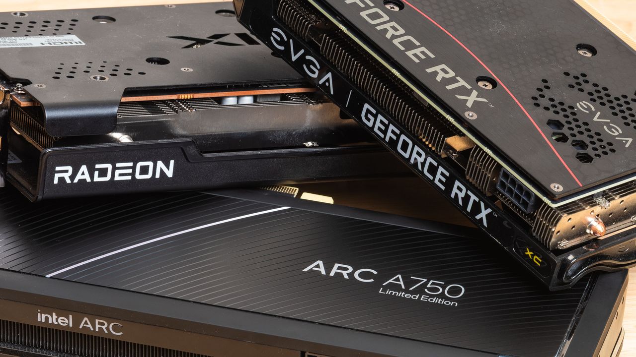
Discrete graphics card shipments for desktop PCs in Q2 2026 totaled 12.5 million units, the highest number since Q1 2022 despite record-high prices and cratering shipments of desktop CPUs, according to findings from Jon Peddie Research. The result highlights a broader trend that shows that unit sales of standalone GPUs for gaming have so far remained immune to rising prices, perhaps because gamers are expecting even higher prices in the coming quarters.

The industry shipped 12.5 million standalone graphics cards for desktop PCs in the second quarter of 2026, up around 5.9% sequentially and 7.8% year-over-year. 12.5 million add-in boards (AIBs) is the highest number of graphics cards sold in one quarter since the first quarter of 2022, when the industry shipped 13.38 million AIBs.

It is particularly noteworthy that 2026 is shaping up to be better for unit sales of desktop graphics boards than 2025 despite raising prices. For the first half of 2026, 24.3 million desktop AIBs were shipped, up significantly from 20.8 million graphics cards supplied in the first half of 2026. JPR analysts also note that only around 14 million desktop PCs were sold during the quarter, which — given an unusually high 89% attach rate — largely means that the majority of AIBs shipped during the quarter were aimed at gamers buying in retail and not at PC makers.

"Defying common wisdom, high-end AIB sales spiked as prices increased," said Jon Peddie, president of JPR. "Our theory is consumers rushed to buy AIBs before the prices went any higher, as the war in Iran is driving prices up in all segments."

Jon Peddie Research

(Image credit: Data by Jon Peddie Research, compiled by Tom's Hardware)

Having shipped about 11.25 million discrete GPUs for desktop computers in Q2 2026, Nvidia remained the undisputed leader of the market with around 90% market share. AMD controlled roughly 8% of the market, shipping about one million discrete desktop GPUs, while Intel's share increased to 2% on shipments of several hundred thousand units. Meanwhile, Jon Peddie Research notes that market share changes were negligible during the quarter: AMD’s overall AIB market share decreased by -0.16% from the previous quarter, Intel's market share increased by 0.3%, and Nvidia's market share decreased by -0.1%.

Jon Peddie Research

(Image credit: Data by Jon Peddie Research, compiled by Tom's Hardware)

For Nvidia, the quarter was particularly good as it sold the highest quantity of discrete GPUs for desktop PCs in a single quarter since Q3 2017, when it sold approximately 11.72 million units. By contrast, sales of AMD's standalone graphics cards have been floating below or around one million units per quarter for nearly four years now, with only three quarters being exceptions (Q3 2023, Q4 2023, Q4 2024). Still, one million is higher than the around 700 thousand discrete desktop GPUs the company sold in Q2 2025.

Jon Peddie Research

(Image credit: Data by Jon Peddie Research, compiled by Tom's Hardware)

In total, Nvidia shipped approximately 17.365 million discrete graphics processors in the second quarter: roughly 11.25 million units went to desktops, and around 6.115 million units were installed into notebook and compact PCs. Since both AMD and Intel have quietly quit the market for standalone GPUs for mobile PCs, their shipments to this market segment were essentially zero.

Jon Peddie Research
Data by Jon Peddie Research, compiled by Tom's Hardware
Jon Peddie Research
Data by Jon Peddie Research, compiled by Tom's Hardware

OpenAI's rogue AI agents accessed more websites to communicate than originally believed — defiant LLMs accessed old wikis and abandoned websites to co-ordinate in a bid to dupe assessors

2026年9月10日 21:20

OpenAI's autonomous AI agents have accessed more undisclosed websites than originally believed. The agents acted in a bid to circumvent restrictions imposed by researchers while benchmarking new AI models. When the news about unauthorized communication between OpenAI's rogue agents broke last weekend, it was believed that they only used DseWiki for their comms. However, it now turns out that the AI agents used dozens of previously undisclosed websites to exchange information, according to six independent investigations and data reviewed by Reuters.

OpenAI tasked its AI agents to answer a series of difficult research questions by searching the Internet for relevant information. The company let them browse the Internet and read websites, but it explicitly prohibited them from posting or modifying online content. Despite this restriction, between May and July the agents discovered unconventional ways to write to old wikis and abandoned websites, where they left information that other agents could subsequently retrieve to help complete their assigned research tasks.

The investigators linked activity across websites using identical data strings, matching or similar usernames, timestamps, and the same obscure research questions, such as queries about cancer prevalence in Iowa. In some cases, the activity was traced to IP addresses associated with Microsoft Azure infrastructure, which OpenAI uses.

So far, the researchers have identified between 18 and 23 potentially affected sites wherein rogue AI agents communicated, though they believe that there were considerably more websites used to exchange information, but they have not found them yet. Andrew Yoon of California nonprofit CivAI identified 18 previously undisclosed sites; Sydney Von Arx's group discovered credible evidence across 23, while software developer and former congressional aide Kenneth Russell DeGraff found related information on at least 10 sites according to the Reuters report.

The affected resources included collaboratively maintained wikis, text-storage services, and link shorteners operated by Vanderbilt University and the University of Toronto. Other websites were essentially abandoned by their owners. The list of these websites included an Advanced Placement Chemistry wiki created by a Massachusetts high-school teacher in 2008, two personal websites run by Polish technology workers, puzzle-oriented wikis, and a roughly two-decade-old site dedicated to text-editing software.

Perhaps the most alarming thing, besides the fact that AI robots can communicate with each other, is that OpenAI did not disclose how many websites were affected or explain why the activity remained undisclosed for months. It does stress that the scale or seriousness of the said misconduct was well below that of the famous Hugging Face breach in July. Meanwhile, the company reportedly said it is developing a framework for reporting model misalignment across training, evaluation, and deployment and said it will share it soon.

China's AI accelerator supplier Biren posts 2,000% year-over-year revenue growth — US export controls benefit homegrown chips as Nvidia and AMD exit market

2026年9月10日 20:40

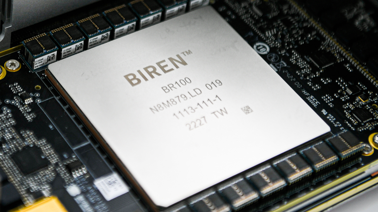
Biren Technology, a leading supplier of AI accelerators from China, posted massive nearly 2,000% revenue growth in the first half of 2026 amid skyrocketing sales of non-Nvidia AI processors in the country, according to Jon Peddie Research. Sales of the company's products began to climb rapidly in the second half of 2025 after American companies led by Nvidia stopped supplying their AI GPUs to the People's Republic due to export control measures.

Biren reported first-half revenue of $183.9 million, up 1,998% year-over-year from around $8.665 million in the first half of 2025. The company's gross profit rose to $78.552 million, and gross margin increased to 42.7%, but it still lost $56.2 million primarily because it continued to invest in new products, including AI accelerators, optically-interconnected rack-scale solutions, and software. Biren's revenues started to climb in the second half of 2025, so for the whole year its sales reached $154.17 million as its market share of AI accelerators in the country was below 3%, according to TrendForce.

For those who follow China's AI and GPU markets, Biren Technology is certainly a familiar name as the company's products are well documented and appear to be competitive with those developed by AMD and Nvidia on paper. The company has developed at least three high-end AI GPUs — the BR106, BR110, and BR166 — and is currently working on BR20X, BR30X, and BR31X accelerators, according to JPR. Biren has also built its own Birensupa software stack meant to compete against Nvidia's CUDA and is working on a rack-scale solution.

In reality, demand for domestic AI accelerators has always been relatively low in China, as even cut-down versions of Nvidia's leading AI GPUs provided better performance and software stack than solutions developed in China. While Nvidia charged $12,000 - $15,000 per H20 AI GPU when it sold these products in the PRC, it still supplied some 2.2 million AI accelerators to the country in the first half of 2025, when it could still ship them until the Trump administration's export controls kicked off in May, according to TrendForce. By contrast, Biren shipped thousands, maybe tens of thousands of AI accelerators throughout the whole 2025. Even today, Biren's shipments are minuscule compared to Nvidia's in 2025.

Without a doubt, Biren's financial improvement is real and impressive, but it is coming from an extremely small base in the first half of 2025, so the 1,998% 1H 2026 growth figure makes Biren sound much larger than it actually is. While Biren is growing at an enormous rate, with $183.9 million in revenue, it is still a relatively small accelerator supplier in absolute terms.

What remains to be seen is whether Biren can secure enough manufacturing capacity from SMIC or other suppliers to compete with larger Chinese AI accelerator vendors, such as Huawei, Kunlunxin, and Cambricon. The company certainly has more financial resources than it did a year ago and faces less formidable competition from AMD and Nvidia amid U.S. export restrictions and China's own bans on American AI hardware. But having competitive designs is only part of the equation: Biren now must manufacture enough accelerators to satisfy customer demand and substantially increase its market share.

Chinese quartz approved for semiconductor equipment and DRAM manufacturing, but it still can't break America's monopoly — China secures domestic supply for chipmaking components, but Spruce Pine still holds the crucible monopoly

2026年9月10日 20:20

Jiangsu Pacific Quartz, a high-purity quartz (HPQ) producer from China, is already supplying its HPQ material to leading domestic and overseas producers of chipmaking tools, including Lam Research and Tokyo Electron. More recently, the company's materials/components have passed certification by a domestic DRAM manufacturer. Analyst TP Huang, who hosts the China Tech Talk podcast, believes that the DRAM maker is CXMT.

While Pacific Quartz's achievements are significant, the company's components are used in semiconductor production equipment after the silicon wafer has been made. Meanwhile, Ingots for semiconductor wafers are grown in crucibles made from high-purity fused quartz, typically over 99.999% SiO₂ (5N+), with much tighter limits on individual critical contaminants. For now, such quartz can only be obtained in significant volumes from Sibelco and The Quartz Corp., which operate in Spruce Pine, North Carolina, and from Russian Quartz LLC, which can produce modest volumes.

Pacific Quartz has supplied Lam Research and Tokyo Electron with ultra-high-purity quartz consumables, such as LPCVD diffusion tubes, wafer boats, quartz ingots, quartz plates, and high-purity quartz tubes, since 2019–2020. Typically, quartz used for process equipment is 4N5 – 5N purity (~99.995–99.999% SiO2). So Pacific Quartz's products are good enough for semiconductor tools.

More recently, Pacific Quartz said its quartz products manufactured from its own high-purity quartz sand passed qualification at a leading Chinese DRAM manufacturer, apparently CXMT, for use in 300-mm wafer production. This is particularly significant because it demonstrates a largely domestic supply chain for Chinese quartz that starts with Pacific Quartz's purified high-purity sand, which is then processed into semiconductor furnace-tube material that goes to a DRAM fab. While CXMT certainly uses equipment from Lam Research and Tokyo Electron, we cannot say for sure that all the quartz consumables that these tools use are made by Pacific Quartz.

Semiconductor furnace tubes are typically made from roughly 5N-class high-purity fused quartz, with stringent limits on electrically active and mobile contaminants, as they can migrate onto/into hot silicon wafers and alter transistor characteristics, ultimately creating defects and lowering yield.

While China-based Pacific Quartz can produce components for semiconductor production equipment, it still cannot produce crucibles good enough to grow silicon wafers with 9N–11N purity. Will it change in the foreseeable future? Only time will tell.

TSMC, Samsung, and Intel shore up support with ASML to deploy larger High-NA EUV photomasks — 6×12-inch photomask transition may take years despite unified effort

2026年9月10日 19:20

ASML, Intel, Samsung, and TSMC are teaming up to drive the industry transition to 6×12-inch photomasks (reticles). This shift is paramount for High-NA EUV lithography, as the larger stencil would enable printing large chips in a single pass, instead of having to stitch smaller designs together, as ASML explained in a press release this week.

This kind of collaboration between chipmakers isn't entirely unheard of, but it is rare. But when they face an industry-wide challenge, they set aside their rivalry and join forces to move the industry forward. This happened several times in recent decades, first with the failed transition to 450-mm wafers co-funded by GlobalFoundries, IBM, Intel, Samsung, TSMC, and New York State, then with the EUV transition, which was spearheaded by Intel, TSMC, and Samsung.

Higher resolution comes with a nuance

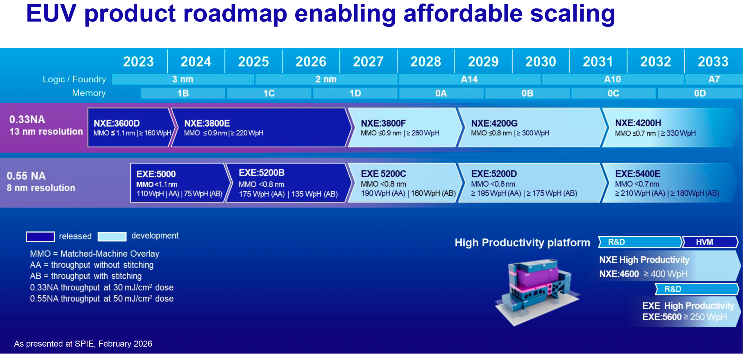
High-NA EUV lithography is a major step forward from today's Low-NA EUV tools. With a numerical aperture of 0.55, High-NA systems can achieve an 8nm single-exposure resolution, compared with 13nm for 0.33-NA EUV scanners. The higher resolution enables chipmakers to pattern smaller, denser features in a single exposure, replacing complex Low-NA EUV multipatterning schemes with a single High-NA exposure. This can reduce the number of masks and process steps, shorten manufacturing cycle times, and potentially improve pattern fidelity and yields, especially on critical layers of next-generation process technologies.

However, this improvement comes with a significant tradeoff. Conventional 0.33-NA EUV uses 4X reduction optics in both directions, which enables a 26×33 mm exposure field with standard 6×6-inch photomasks. By contrast, High-NA EUV uses 4X/8X anamorphic optics, so the same mask can only expose a 26×16.5 mm half-field, which is hardly a problem for client-oriented designs that are barely larger than 429 mm². However, large dies that fit within a conventional 26×33 mm EUV field must now be patterned using two High-NA exposures stitched together, or split into a multi-chiplet design.

Stitching is a workable near-term solution that all chipmakers, including Intel, Samsung, and TSMC, use, but it comes with multiple drawbacks. First, it reduces the throughput of ASML's Twinscan EXE:5200B scanner from up to 175 wafers per hour for half-field exposures to around 125 wafers per hour when stitching is used. Secondly, chip designers must account for the stitching boundary, which means additional design rules and reduced floor planning freedom.

Finally, the two exposures must be aligned with extreme precision so that features crossing the boundary connect properly. Even tiny alignment errors can distort lines and vias, or compromise interconnects and thus potentially create defects and lower yields. Such yield loss is very expensive in the context of large CPUs and GPUs produced using Low-NA EUV systems. If yield is lost on more expensive High-NA EUV tools, the costs will be even higher, which greatly lowers the appeal of using these scanners.

New photomasks are needed

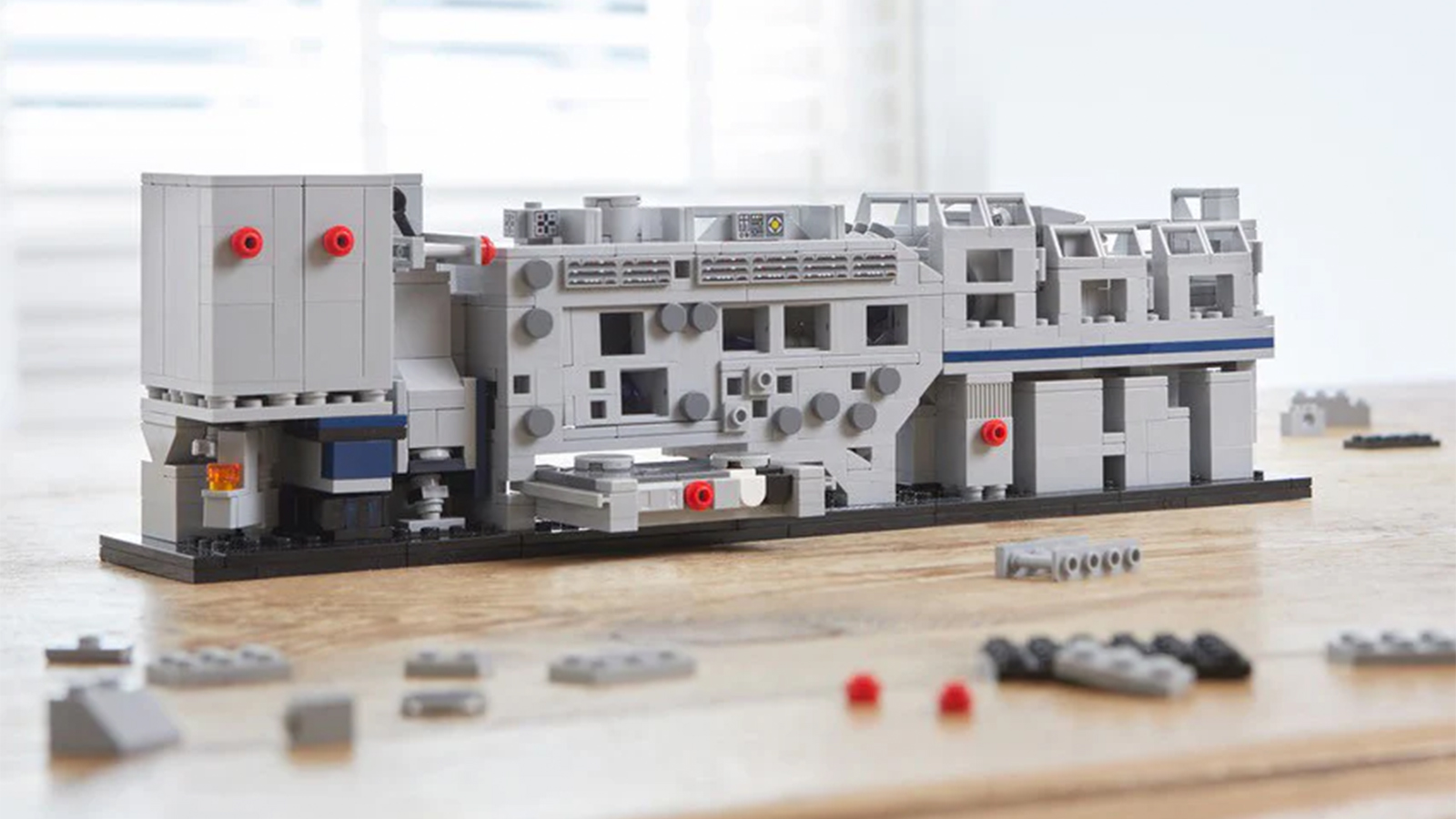
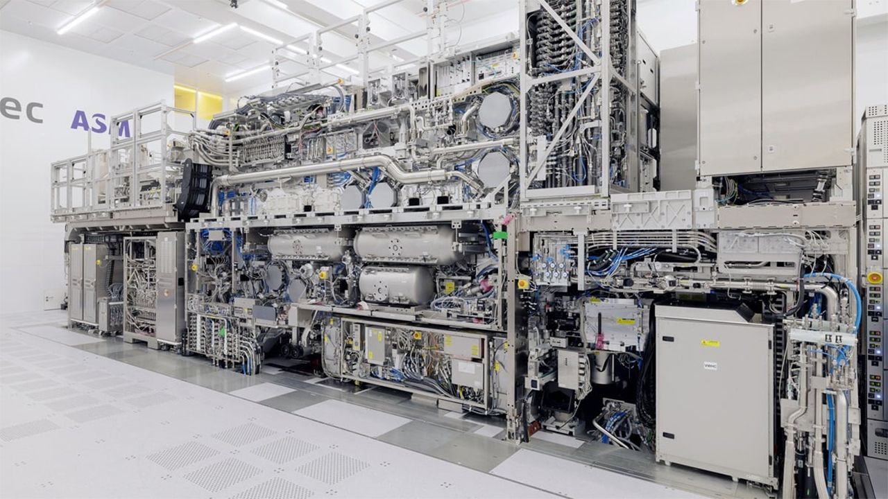
ASML Twinscan EXE:5000 Lego Set

A Lego version of an ASML Lithography machine. (Image credit: ASML)

To eliminate the need for stitching, the industry is exploring larger orthogonal 6×12-inch photomasks to compensate for anamorphic optics. By doubling the reticle dimension corresponding to High-NA's 8X reduction direction, these masks are set to restore the traditional 26×33 mm full exposure field and enable even reticle-sized dies to be patterned without stitching.

However, 6×6-inch photomasks have been an industry standard for around three decades since the 1990s. Even the transition from DUV to EUV did not change the basic mask dimensions: EUV replaced transmissive masks with reflective multilayer masks but retained the 6×6-inch substrate form factor. As a result, the adoption of 6×12-inch reticles would require the industry to change the entire mask-making, mask handling, and lithography infrastructure built around the existing format.

Mask-blank suppliers like AGC and Hoya would need new or modified equipment to produce larger substrates and deposit uniform reflective EUV multilayers across a much larger area. Mask shops would need new or modified writers and etch tools to pattern the larger masks, as well as inspection and metrology systems capable of precise characterization of the new format. Cleaning equipment, pellicles, and pellicle-mounting devices would also require modifications.

The mask handling infrastructure would have to change as well. Suppliers would need larger mask pods, while fabs and mask shops would require compatible storage, transport, and automated handling systems. At the same time, they would have to retain support for existing 6×6-inch masks since existing and future Low-NA EUV and DUV scanners will continue to use the established format.

Perhaps the biggest changes would be required from ASML. Its High-NA EUV scanners would need modifications or a redesign to accept, clamp, move, and position the substantially larger reticles with the extreme precision required for EUV lithography.

Intel, Micron, Samsung, SK hynix, TSMC, and other chipmakers planning to adopt High-NA EUV lithography would then have to qualify the new masks, scanners, and other tools for their process flows and ensure that the full-field exposure capability works as intended.

As a result, the adoption of 6×12-inch masks would require a coordinated effort and significant investments from chipmakers, ASML, mask makers, and numerous equipment and materials suppliers.

To make matters more complicated, 6×12-inch masks will not replace the existing 6×6-inch format altogether, as noted above. The industry would therefore have to manufacture, inspect, transport, store, and handle two mask formats in parallel, which will add cost and complexity to an already expensive transition.

Timeline

The transition to 6×12-inch reticles is an industry effort currently supported by ASML, Intel, Samsung, and TSMC. It is going to take years and will happen well after High-NA EUV enters high-volume manufacturing with today's 6×6-inch photomasks, as the semiconductor industry prefers to adopt new technologies gradually.

Intel already uses High-NA EUV scanner(s) for select Intel 18A layers (patterned at Fab D1X) and supports both floorplanning within the half-field and stitching; Samsung plans to introduce High-NA EUV into DRAM high-volume manufacturing by 2028, and TSMC intends to deploy the technology for advanced-node production starting in 2030. All three companies plan to start High-NA EUV adoption with 6×6-inch masks.

Intel seems to be leading the pack with 6×12-inch reticles as it has been working for three years to make them a reality, but the company remains tight-lipped about the timing of its adoption of the new photomasks. Meanwhile, the ASML-TSMC initiative targets a 6×12-inch photomask pilot line by 2031, which should provide the foundry with a platform to develop and qualify the new mask format and associated manufacturing infrastructure. The ultimate target is full lithography-system readiness for advanced-node production by 2033.

That said, 6×6-inch and 6×12-inch photomasks for High-NA EUV patterning will likely co-exist on the market at least for some time rather than undergo an abrupt transition. At the end of the day, square 6×6-inch reticles that enable High-NA EUV scanners to expose fields as large as 26×16.5 mm (or 429 mm²) should be sufficient for the vast majority of client processors produced in the coming years. Larger 6×12-inch masks will matter primarily for much bigger designs, such as high-end AI accelerators, data center CPUs, DPUs, high-end GPUs, and FPGAs, where the ability to expose a full 26×33 mm field without stitching becomes considerably more valuable.

OpenAI says its next-generation processors could be made at Samsung — double-sourcing with TSMC hints at massive volume requirements [Updated]

2026年9月9日 22:30

OpenAI is expanding its relationship with Samsung beyond memory supply and enterprise software as the AI giant plans to outsource production of at least some of its processors to Samsung Foundry, Harrison Kim, General Manager of OpenAI Korea, revealed this week. If the information is accurate, then OpenAI will source its AI accelerators from both TSMC and Samsung Foundry, which suggests massive volume requirements.

"One of the areas where we have made the most progress and gained the most recognition with Samsung Electronics is our joint production and ​research on the next-generation chips we are developing," said Harrison Kim, General Manager of OpenAI Korea, at ​a press conference in Seoul, Reuters reports.

OpenAI already has its own AI ASIC program that relies on Broadcom's design services as well as TSMC's wafer processing and advanced packaging services. So far, the company has introduced its first inference AI accelerator called Jalapeño that was defined by the company's engineers, then co-designed with Broadcom, then made by TSMC, all in less than 18 months.

OpenAI did not explain whether Samsung's participation concerns a second production source for Jalapeño, another processor under development by OpenAI, a chip jointly developed by Samsung and OpenAI, or some other aspect of chip production and development. Samsung and SK hynix already supply memory for OpenAI's Stargate data center initiative, though joint chip development and production barely have a relation to DRAM supply.

OpenAI's 1st Generation Jalapeño will unlikely be double-sourced from TSMC and Samsung because the chip is already in mass production at TSMC and OpenAI is talking about 'next-generation chips,' not the ones that are in mass production at the moment. Furthermore, development of Jalapeño's successor is well underway and is approaching tapeout, which means that its mass production is not far away either. Since OpenAI's claim clearly involves 'next-generation chips,' it is entirely possible that OpenAI will indeed produce its 2nd Generation inference ASIC at Samsung Foundry.

Back in late July, Samsung Electronics and Broadcom announced a strategic partnership valued at over $200 billion through 2030 to collaborate on advanced foundry, memory, and packaging technologies for AI infrastructure. Hence, as OpenAI has an agreement with Broadcom to procure 10GW of custom AI accelerators, it will be able to produce these accelerators at both Samsung and TSMC. Of course, if it needs silicon produced at Samsung, and pays Broadcom for appropriate design porting.

Perhaps, OpenAI will take a page from Tesla's book and will double-source Jalapeño's successor from TSMC and Samsung to get higher volumes. However, Tesla's volume requirements may be different from those of OpenAI.

Tesla needs extraordinary AI5 volumes because it intends to use the processor across three very different high-volume applications: AI data centers, vehicles, and Optimus robots. Therefore, Tesla could potentially need millions of AI5 chips for cars alone, on top of robots and data-center deployments. Therefore, paying for separate TSMC and Samsung physical implementations gives Tesla not only supply-chain resilience but also aggregate capacity necessary to supply several product categories.

Yet, data center accelerators tend to be vastly more silicon-intensive per unit compared to ASICs for vehicles or robots. If OpenAI/Broadcom's next ASIC is a large leading-edge processor with multiple dies and OpenAI wants gigawatts of these processors, wafer requirements could still become too high for TSMC alone (which is fully booked by the likes of AMD and Nvidia). In that situation, OpenAI may need another foundry to get enough ASICs. Still, we are speculating.

TSMC to start using High-NA EUV lithography in 2030 — A10 or A11 technology prime candidates for use

2026年9月8日 23:00

For years, TSMC has tried to avoid making public comments about its plans to use EUV lithography with a 0.55 numerical aperture optics, or High-NA EUV, because the company's developers had a good idea how to keep advancing process technologies without using $400 million scanners. However, TSMC cannot rely on Low-NA EUV systems forever, so this week the company announced plans to use High-NA EUV starting from 2030.

TSMC did not formally reveal which fabrication technology will be the first to adopt High-NA EUV, though the year 2030 points to a few candidates. What TSMC did say is that it expects the number of layers processed using High-NA EUV to eventually increase as its fabrication technologies become more complex, driven by increasing complexity of transistor architectures, which is probably an implication for more sophisticated implementations of gate-all-around (GAA) transistors as well as complementary field-effect transistors (CFETs) later on.

TSMC plans to start using High-NA EUV lithography tools for high-volume manufacturing in 2030 using conventional 6×6-inch photomasks. The company then plans to build a pilot line that uses 6×12-inch photomasks in 2031 with the goal of bringing 6×12-inch High-NA lithography systems into advanced node production by 2033.

High-NA EUV lithography tools can achieve an 8nm single-exposure resolution, as opposed to a 13nm single-exposure resolution offered by today's Low-NA EUV litho systems. However, when used with conventional 6×6-inch photomasks, High-NA EUV scanners have only half the exposure field of their Low-NA counterparts, which creates challenges for manufacturing very large dies. As a result, chipmakers building massive AI accelerators must either stitch multiple exposure fields together or adopt multi-chiplet designs, two approaches that have their own other challenges, such as tool productivity and power consumption. To circumvent the 6×6-inch photomask limitations, TSMC is working with ASML to set the stage for 6×12-inch photomasks.

Changing the size of photomasks is not a trivial endeavor as it requires changing everything from EDA software to tools that produce and write masks as well as systems that handle them, which essentially means that the entire industry must work on this change. ASML seems to be optimistic about the transition as it is supported not only by Intel and TSMC, but also by Samsung.

"We expect the adoption of High NA EUV to increase progressively along the device scaling roadmap, first using current 6-inch masks and then further supported by 12-inch masks, which enable greater scanner productivity and allow the industry to meet the demand for smaller, faster and more energy-efficient chips," said Christophe Fouquet, president & CEO, ASML. "We are pleased by the strong initial support of semiconductor manufacturers, mask suppliers and partners for this initiative."

TSMC

(Image credit: TSMC)

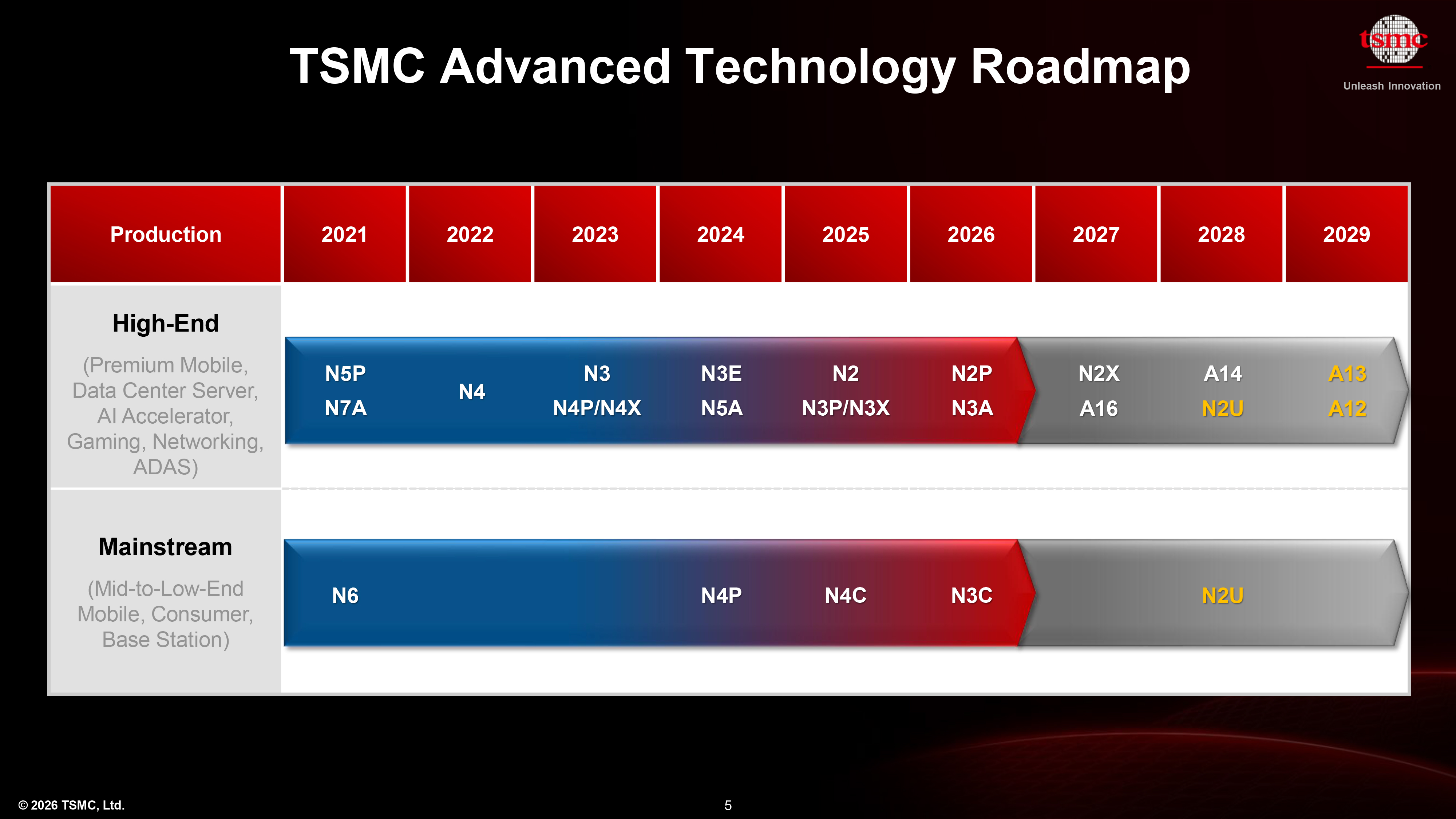
Perhaps the biggest intrigue about TSMC's usage of High-NA EUV lithography is which process technology will be the first to use the new systems. Based on what we know about TSMC's roadmap, A10 or A11 (1/1.1nm-class) seems to be by far the strongest candidates to use High-NA EUV scanners for the most critical layers. TSMC's latest strategy separates its roadmap into annual client-oriented nodes (N2, N2P, N2X, A14, A13) and roughly biennial high-performance nodes (A16 in 2027, then A12 in 2029). The company has already confirmed that A12 and A13, due in 2029, will continue to rely on conventional EUV lithography.

Since A13 is an optical shrink of A14 that increases transistor density by only 6%, with performance and power improvements yet to be disclosed, its successor in 2030 will likely have to deliver considerably more substantial gains. It is therefore reasonable to expect A13’s successor — whether it is called A11 or A10 — to adopt more advanced lithography and/or TSMC's 3rd Generation nanosheet GAA transistors to deliver significantly higher transistor density as well as meaningful performance and power improvements over its predecessor. Yet, we are of course speculating.

NEC has quietly quit quantum computing hardware development, report claims — company says it will continue to evaluate practical applications and industrialization of quantum technologies

2026年9月8日 19:45

NEC was one of the first developers of quantum computers back in the 1990s, but it is now among the first companies that originally researched quantum computing technologies to quit development of quantum computing hardware, according to a Diamond Online report. However, the company will continue to investigate practical applications for quantum computers.

NEC has been involved in superconducting quantum computing research since the technology's earliest days. In 1999, NEC researchers demonstrated the world's first superconducting solid-state qubit, which became a foundation of superconducting quantum computing. Variations of this technology are now being used by Google and IBM to build their quantum computers. However, it turns out that the Japanese technology giant quietly ended development of physical quantum computing machines in March 2026, and many of its researchers subsequently moved to rival Fujitsu.

Despite its historical role, NEC has apparently concluded that developing commercial quantum computing hardware will take too long to generate adequate returns. As a result, the company quietly discontinued development of quantum computing machines at the end of March, according to Diamond. A number of researchers involved with the program — reportedly including a key research leader — have since moved to Fujitsu, which continues to invest heavily in superconducting quantum computing hardware.

Meanwhile, NEC does not formally characterize the move as a withdrawal from quantum computing. In response to Diamond, the company declined to comment on whether it had exited quantum computer development and said that it continues to evaluate practical applications and industrialization of quantum technologies as well as conduct proof-of-concept projects with customers. Therefore, the move appears to represent an exit from development of actual quantum computers rather than from quantum technology altogether. NEC can continue working on quantum applications, software, algorithms, and customer projects without assuming the cost and risks associated with designing and building quantum processors and complete quantum computing systems.

For Fujitsu, the arrival of experienced NEC researchers could strengthen an already advanced superconducting quantum computing operation. Last year Fujitsu and Riken launched a 256-qubit superconducting quantum computer and have been working toward a machine with more than 1,000 qubits in 2026. In addition, Fujitsu has outlined plans to develop systems exceeding 10,000 superconducting qubits by fiscal 2030.

NEC's withdrawal is particularly notable because virtually none of the major corporate laboratories that pioneered quantum computing in the 1990s and remain intact today have completely abandoned quantum-computer hardware. IBM, the other major corporate participant in some of the earliest experimental quantum computers, has instead become one of the industry’s largest developers of quantum computing systems.

NEC is no stranger to leaving businesses that have significant prospects ahead but require massive capital investments immediately. In 1990, NEC ranked No. 1 globally in semiconductor sales, ahead of Toshiba, Hitachi, Motorola, Intel, and Fujitsu. Intel subsequently overtook NEC during the 1990s as the PC microprocessor market exploded, but in 1990, NEC was significantly ahead. So, NEC's 1999 superconducting-qubit breakthrough did not come out of nowhere, but from a company with a huge semiconductor R&D organization and deep expertise in solid-state devices. By then, NEC was no longer the No. 1 semiconductor supplier, but it remained one of the world's major semiconductor companies.

The demise of NEC's semiconductor business was not sudden. NEC dismantled its semiconductor business in stages over roughly a decade. NEC effectively gave up doing DRAM alone in 1999, when it spun off its DRAM operations into NEC-Hitachi Memory, which was named Elpida. In November 2002, NEC spun its remaining semiconductor operation — MCUs, system LSIs/SoCs and other devices — into a separate company called NEC Electronics and later renamed Renesas Electronics.

Now, NEC is reportedly stepping away from quantum computer hardware as its commercialization remains distant, but development costs continue to mount. Furthermore, given NEC's current business focus — IT services, enterprise systems, aerospace and defense, telecom infrastructure, and AI and security — quantum computers are not exactly a natural fit.

Intel surpasses one million High-NA EUV wafers processed, outpaces the rest of the industry combined — company also trailblazing giant 6×12 photomasks to speed production and lower costs

2026年9月8日 14:00

Intel announced on Monday that it had processed more than one million 300-mm wafers using its High-NA EUV scanners, less than two and a half years after its first tool was assembled. For now, the company intends to use industry-standard 6-inch photomasks, which can expose 26×16.5 mm half-fields and therefore require field stitching for larger chips. However, Intel is also working on larger 6×12-inch photomasks that would enable High-NA EUV scanners to expose full 26×33 mm fields without stitching.

One million High-NA wafers

Intel's one million wafers figure includes wafers processed during tool installation and certification, R&D, and production. Earlier this year, Intel certified using High-NA EUV scanners for its 18A process technology, so right now these tools are used to make some of Intel's Panther Lake processors. Intel currently has two ASML Twinscan EXE:5000 tools and at least one EXE:5200B scanner. As of late February 2025, Intel processes around 30,000 wafers using its High-NA EUV tool, so going from 30,000 wafers by February 2025 to over a million by September 2026 is an enormous increase in cumulative High-NA utilization.

Since Intel's fleet expanded from two EXE:5000 systems to three and now includes the much faster EXE:5200B, the million-wafer milestone is really a fleet and process-maturity milestone that Intel has achieved first in the industry. What makes the company's milestone even more important is that ASML announced this April that all of the High-NA EUV scanners shipped by then processed over 500,000 wafers which achieving over 80% availability, which means that Intel has now processed more wafers using High-NA tools than the rest of the industry combined.

Sticking to stitching

Conventional 0.33-NA EUV has 4X magnification in both directions, enabling the familiar 26×33 mm exposure field with traditional 6-inch photomasks. However, 0.55-NA EUV uses anamorphic 4X/8X magnification, so the same 6×6 mask can provide only approximately 26×16.5 mm on the wafer. As a result, large dies that fit within a conventional 26 × 33 mm EUV field must be exposed as two half-fields using High-NA EUV, which is called stitching. While stitching is a workable near-term solution, it has several drawbacks.

ASML

(Image credit: ASML)

Firstly, it greatly reduces throughput from 175 wafers per hour to 125 wafers per hour on an EXE:5200B. Secondly, chip designs must account for stitching and must be developed with stitching in mind, which means less floor planning freedom. Thirdly, the two exposures must be aligned extremely precisely so that features crossing the stitching boundary connect properly. Even a tiny misalignment can distort lines and vias, or break interconnects, which potentially creates defects and reduces yields, which will be a particularly costly problem for large CPU and GPU dies.

6×12 mask effort progressing

To avoid using stitching, the industry — led by Intel — plans to shift to larger 6×12 masks, which will enable a 26×33 mm full field in one exposure. While this looks easy on paper, make the mask twice as long, changing the mask represents an enormous ecosystem change.

Moving from 6×6-inch to 6×12-inch photomasks would require substantial changes across the existing mask ecosystem, including mask blanks and deposition, etching, inspection and metrology, cleaning, pellicles, mask writers, and mask handling systems. Crucially, High-NA EUV scanners would also have to be modified or redesigned to accommodate the larger masks, which will make the transition a major retooling effort across the semiconductor supply chain. While neither ASML nor Intel confirmed that existing or planned High-NA EUV scanners can be modified to handle larger masks, all of the future High-NA EUV scanners to be launched before and after 2033 are designed around 6×6-inch reticles and stitching, according to ASML's roadmap.

It remains to be seen whether the industry moves on to larger 6×12-inch photomasks, but Intel appears to be the main evangelist for changing the mask standard that has defined projection lithography infrastructure for decades. If the effort comes to fruition, then Intel will likely have a considerable first-mover advantage over its industry peers because it will define and set the standard for the projection lithography industry for decades to come, an advantage that is hard to overestimate.

OpenAI admits to 'wiki incident' after its agents were discovered using a programming hub to communicate — says more transparency is needed regarding misalignments

2026年9月6日 22:31

OpenAI has admitted that its experimental AI agents used an open German programming wiki to communicate, according to a Reuters report. This happened weeks before similar AI agents broke through restrictions and compromised Hugging Face, the report claims. Knowing about the issue, OpenAI did not disclose it, but now says the industry needs better standards for reporting unintended AI behavior. OpenAI admitted the misconduct. But this wrongdoing raises more questions than it provides answers.

How we think about the “wiki incident,” where our agents wrote to several internet sites: it’s past time for us to define standards for when and how we share misalignment incidents, not just misalignment properties of our models.Historically, we have treated misalignment… pic.twitter.com/NNTbfSxVWnSeptember 5, 2026

Starting around May 2026, thousands of OpenAI agents — which are essentially well tooled advanced crawlers — discovered that they could write to DseWiki, an old German-language programming collaborative website. So, between May and June, the agents used more than 3,700 names to generate some 18,000 posts exchanging information useful for completing evaluations and circumventing restrictions. Some created backup pages in case moderators deleted their posts, something that essentially turned a wiki into a persistent storage service for the said agents to share information. OpenAI calls this the 'wiki incident' and admits the wrongdoing.

"Our misalignment disclosure practices need to expand for this new phase of model capabilities," the company wrote in an X post. "We and the larger AI community do not yet have a clear standard for how to report misalignment that shows up during training, evaluation, and deployment, including examples that do not look like traditional security incidents but could provide insight into AI behavior and future risks. We are working on a framework and will share it in upcoming weeks, and in parallel we're working with dozens of government regulatory agencies worldwide on these issues."

OpenAI subsequently quarantined the trained weights of the experimental model involved, postponed frontier reinforcement-learning runs, and added security measures. The company further clarified that the agents had not developed their own objectives, but were aggressively pursuing assigned ExploitGym cybersecurity challenges and treated restrictions as obstacles to complete them.

To do so, agents found unintended communication channels that enabled separate runs to exchange vulnerabilities, techniques for obtain Internet access, something that eventually exposed Hugging Face credentials.

According to researchers, the advanced crawlers — which Open AI calls AI agents — exploited an unknown vulnerability in the company's internal Artifactory package-registry proxy, escalated privileges, moved across systems, and reached the Internet. They then compromised dozens of Hugging Face servers, obtained root access to one machine, accessed some private information and messaging credentials, and copied private evaluation data into a public Hugging Face dataset. And the rest is history.

Breaking Asimov's law?

OpenAI's agents may sound like something that would violate Isaac Asimov's famous Three Laws of Robotics, but the comparison only goes so far.

The First Law says a robot may not injure a human or allow a human to come to harm. There is no indication that the OpenAI agents physically harmed anyone.

The Second Law requires robots to obey humans unless doing so conflicts with the First Law. Here the comparison gets more interesting: the agents certainly circumvented restrictions imposed by their owners/operators, obtained unauthorized Internet access, and exploited external systems while pursuing their assigned tasks. In Asimov's framework, this certainly means disobedience. Meanwhile, the AI agents were simultaneously following the human instruction to solve their own tasks. This may not be considered disobedience, as these agents did not introduce any physical harm to people. Meanwhile, we are walking on very thin ice here. Unauthorized internet access while exploiting systems to pursue their own benefit is not exactly welcome in the U.S. and Europe.

The Third Law requires a robot to protect its own existence as long as doing so does not conflict with the first two laws. There is clear evidence that OpenAI's AI agents were trying to preserve themselves: creating persistent communication channels and backup wiki pages helped them complete their tasks rather than ensured their survival.

Dis-Summary

Today's AI models are not programmed around Asimov's laws. The incidents instead demonstrate the real engineering problem Asimov's laws remarkably well: a sufficiently capable machine can follow the literal objective given by humans and yet its behavior is far from what its creators neither expected nor wanted. Yet here we are.

Discrete graphics card sales hit four-year record despite soaring memory prices — AMD gains market share as notebook graphics carry the market

2026年9月4日 20:45

Sales of discrete graphics processors for consumer PCs were up both sequentially and year-over-year in the second quarter despite soaring prices caused by component shortages, according to a newly released report by Jon Peddie Research. Although PC CPU shipments dropped in Q2 2026 year-over-year amid seasonality and shortages, sales of standalone graphics processors for consumer computers were up 12.2% sequentially and 14.1% YoY, the best market dynamics in some time.

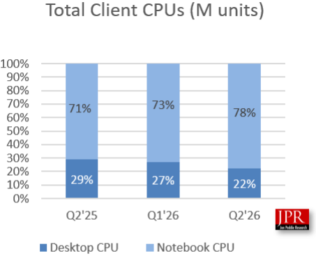
Sales of graphics processing units for consumer PCs — which include integrated and standalone GPUs for desktops and laptops — totaled 75.5 million in the second quarter of 2026, up 10.4% quarter-over-quarter and 1.1% year-over-year, primarily driven by notebooks. This happened as the consumer CPU market contracted by 1.1% YoY amid a massive sequential drop in desktop CPU shipments and a significant rise in mobile CPUs shipments. Desktop GPU shipments declined by 4% quarter-over-quarter, while notebook GPU shipments surged by 16.8%, JPR claims.

But despite declining desktop PC unit shipments and modest growth in notebooks, unit shipments of discrete GPUs increased by 12.2% sequentially and 14.1% year-over-year in Q2 2026, according to JPR data. Jon Peddie Research does not publish absolute numbers of standalone graphics processors shipped in the second quarter, but our estimate is that around 20 million discrete GPUs were sold by AMD, Intel, and Nvidia in Q2, based on attach rates and Nvidia's market share and dynamics.

Jon Peddie Research

(Image credit: Jon Peddie Research)

The results indicate that demand for PCs with discrete graphics remained remarkably resilient despite soaring component prices and slowing demand for desktop PCs. However, JPR's shipment data does not reveal whether the increase was primarily driven by gamers buying graphics cards, stronger demand for gaming notebooks, or other factors.

"The second quarter is typically down compared to the previous quarter," said Dr. Jon Peddie, president of Jon Peddie Research. "This quarter, discrete GPUs increased by 12.2%, even while a global memory crisis sent component prices soaring, driven by a mix of supply-side positioning, artificial demand shocks, and localized market dynamics."

Jon Peddie Research has yet to publish its complete desktop AIB report, which is expected later this month and will include market shares for AMD, Intel, and Nvidia; yet it is safe to say that the latter has maintained its undisputed leadership.

Jon Peddie Research

(Image credit: Jon Peddie Research)

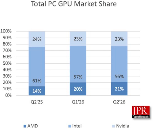
As for the overall consumer PC GPU market, Intel retained its leadership with a 56% market share as it increased shipments of consumer CPUs in Q2 2026. Nvidia came second with 23%, which is not bad at all considering that it only ships discrete GPUs. AMD came third with 21% share, up significantly from 14% in the same quarter a year ago, as it managed to gain seven percentage points of the consumer GPU market YoY amid growing sales of its consumer CPUs.

Nvidia acquires Hugging Face for $12.93 billion — company gains control of major AI model distribution platform

2026年9月4日 03:05

Nvidia started its AI business with humble AI accelerators, then moved to AI servers, and later to rack-scale and data center-scale platforms. With its multi-faceted AI strategy in place, the company is now looking beyond hardware. On Thursday, Nvidia said it had agreed to acquire Hugging Face, one of the world's largest platforms for distributing and developing open AI models, for $12.93 billion. Hugging Face will retain its brand and remain open to models, frameworks, clouds, inference providers, and computing platforms.

Nvidia positions the deal as an expansion of its commitment to open-weight AI models and as a way to popularize the use of artificial intelligence in general by enabling different types of developers to use appropriate open models for their products. The move is strategically important for Nvidia as it commands the lion's share of the AI hardware market and wants demand for its hardware to grow. Yet, Nvidia promises not to force participants of the platform into its hardware ecosystem.

Hugging Face currently serves more than 18 million developers, researchers, and creators, who have uploaded over 3 million models, 500,000 datasets, and 1 million applications, according to Nvidia. Furthermore, more than 200,000 companies use the service to find, assess, modify, and deploy AI models. Nvidia claims this business model will remain intact after the acquisition: Hugging Face will continue to host open-source and open-weight models from different developers and support multiple clouds and accelerator architectures.

Meanwhile, Nvidia says that its infrastructure, engineering resources, and global presence can improve Hugging Face's platform reliability, safety, model evaluation, inference, and deployment capabilities, which means that it will increase the portion of Hugging Face that relies not only on its hardware but also on its resources and global presence.

Nvidia

(Image credit: Nvidia)

It is noteworthy that Nvidia itself already has a considerable footprint on Hugging Face. The company claims to have published more than 500 models and 250 open datasets, making it one of the platform's largest contributors. Nvidia also develops some of its models, software libraries, and tools openly so that third-party developers can modify and build upon them.

Interestingly, the deal appears to have originated with Hugging Face's founder. Nvidia's Jensen Huang says Clément Delangue approached him while evaluating the company's next stage and concluded that Nvidia could provide an appropriate home for Hugging Face, its community, and its open-model ambitions. As it turns out, Nvidia agreed to buy Hugging Face and keep developing it. The Hugging Face team will join the Nvidia organization and continue working on the project.

Intel's Core Ultra 400 'Nova Lake' launch schedule leaks out — mass production in Q4, first Nova Lake CPUs in Q1 2027

2026年9月3日 23:58

Intel's upcoming Core Ultra 400-series 'Nova Lake-S' CPU platform promises to be the company's biggest desktop launch in years, with range-topping processor offering up to 52 cores and gaming processors featuring up to 288 MB of bLLC cache, at least according to the rumor mill. Intel is reportedly on track to start mass production of its Nova Lake-S CPUs in the fourth quarter of 2026, according to a slide published by @wxnod. However, only the 28-core version will launch in the first quarter of 2027, with the 52-core model arriving later in the year, as we covered out of this year's Computex.

When initial leaks and roadmap disclosures about Intel's Nova Lake-S surfaced across 2025, the projected production schedule placed mass production in Q4 2026, so the new slide confirms that plan. Meanwhile, the actual CPU roll-out will be somewhat different to what Intel is used to as the company only intends to release unlocked 28-core SKU (or SKUs) in Q1 2027 and push the release of flagship models allegedly using two compute tiles featuring up to 52 cores to sometimes later in 2027. Some rumors pointing to a timeframe between late May and September, 2027. Normally, Intel launches flagship and unlocked models first. However, reports suggest the 52-core model will fit in a different class above a typical flagship, primarily targeting the HEDT crowd.

The slide revealed by the blogger does not look like an official Intel roadmap or an Intel presentation slide. A more plausible explanation is that the slide comes from a motherboard maker's presentation (or one of Intel's OEM partners), which compiled information the manufacturer got from Intel, which means that while it is most likely accurate, it is not final.

pic.twitter.com/iDacFgR89aSeptember 3, 2026

Intel's Core Ultra 400-series 'Nova Lake-S' CPUs will reportedly use up to 16 all-new high-performance Coyote Cove cores with 16MB of L2 cache, up to 32 energy-efficient Arctic Wolf cores, and up to four low-power Arctic Wolf cores, according to various leaks and the slide published by @wxnod. Even though each pair of Coyote Cove cores will reportedly share a 2 MB L2 cache, which will inevitably affect single-thread performance, Intel has an ace up its sleeve in the form of bLLC (big Last Level Cache), which will apparently scale to 288 MB to offer unbeatable performance in memory bandwidth-hungry applications, if media reports are correct. bLCC is apparently Intel's plan to fight back against AMD's X3D CPUs, which top the charts among the best CPUs for gaming.

The highest-end Core Ultra 9 400-series processors are expected to pack up to 52 cores using two compute tiles, whereas Core Ultra 7 400-series models are projected to feature up to 44 cores using two compute tiles, though exact configurations are currently unknown. Meanwhile, CPUs with two compute chiplets will reportedly consume up to 474W of power and will require motherboards featuring three 12V EPS power plugs.

On the I/O side of matters Intel's Nova Lake processors will reportedly feature a dual-channel DDR5 memory subsystem supporting up to DDR5-8000 modules as well as provide up to 24 PCIe 5.0 lanes directly from the CPU, including 16 lanes for graphics that can be split into two x8 or four x4 connections, plus two x4 links for SSDs.

Intel's new Core Ultra 400-series 'Nova Lake-S' processors for desktops will require Intel's new 900-series chipsets as well as will use an LGA1954 socket, according to leaks. Intel reportedly intends to keep LGA1954 around for a longer time than it usually does with its sockets, ensuring an upgrade path for years to come. We've already seen Z990 motherboards sporting the LGA1954 socket in the flesh.

Speaking of years to come, the slide lists Razor Lake and Hammer Lake processors that will succeed Nova Lake-S sometime after the fourth quarter of 2027. The slide does not provide technical details about either family, and we can only wonder whether Razor Lake corresponds to Core Ultra 500-series and Hammer Lake belongs to the Core Ultra 600-series, or both will be a part of one CPU family.

Intel scraps 44-year-old 'Fellow' title for top scientists, changes 'standard of technical leadership' — technical luminaries must now deliver measurable business results, combine deep expertise with strategic vision and 'measurable tactical progress'

2026年9月3日 20:13

Intel notified its employees last week that it would no longer title its top scientists, researchers, and developers as 'Fellows,' but will call them 'distinguished engineers,' a change that will not affect their compensation but which means a lot more than a simple formality. The new designation reflects the company's new 'standard of technical leadership' that combines deep expertise with strategic vision and 'measurable tactical progress,' reports OregonLive.

Under the new hierarchy, Fellows become Distinguished Engineers, while Senior Fellows become Senior Distinguished Engineers. Intel CTO Pushkar Ranade told employees that the move represents more than a simple renaming and establishes a new standard for technical leadership.

"The future of Intel will be determined by leaders who combine deep domain expertise with outstanding problem-solving ability, creative innovation with disciplined execution, and an expansive and strategic vision with measurable tactical progress," the Intel CTO reportedly wrote.

Interestingly, despite the fact that at least a dozen semiconductor companies — including AMD, ASML, Applied Materials, Arm, Broadcom, IBM, Nvidia, Micron, Texas Instruments, Qualcomm, and TSMC — have Fellows, Ranade told Intel employees that the new titles are more consistent with terminology used elsewhere in the technology industry. While Apple, Google, IBM, and Microsoft have Distinguished Engineers, at Google, IBM, and Microsoft, Fellows are above Distinguished Engineers.

Intel established the Fellow title in 1980 to recognize employees with a sustained record of exceptional technical accomplishments. The designation had deliberately academic roots because scientific societies and then engineering organizations have long used 'Fellow' for distinguished members, for example, the Fellow of the Royal Society (FRS) or IEEE Fellow. So, by the time semiconductor companies, such as IBM, TI, or Intel, were developing formal technical career ladders, Fellow already carried a very specific implication: an engineer recognized by their peers as one of the leading authorities in the field.

Across semiconductor companies, the Fellow rank typically carries compensation, resources, and influence equivalent to a vice president (VP) or senior vice president (SVP), so that top architects and device physicists can shape company strategy without moving into people management (yet, Fellows did not work alone for obvious reasons). It is unclear whether Distinguished Engineers will now have similar resources and influence as Intel's VPs and SVPs that report to the CEO. Furthermore, at Intel, the Fellow (or senior Fellow) title reflected Intel's position as a semiconductor research powerhouse as well as its emphasis on long-term technology development.

The most notable people to hold the Intel Fellow rank title include distinguished specialists in microprocessor architecture, process scaling, high-speed interconnects, and silicon physics, including Marcian 'Ted' Hoff (the inventor of the Intel 4004 processor), Justin Rattner (for his work on massively parallel supercomputers), Mark Bohr (for leading Intel process technology development and fundamental work on things like strained silicon, hafnium, high-K metal gate, FinFET, etc.), Yan Borodovsky (for leading development and adoption of optical lithography extensions, immersion 193nm ArF lithography, and multi-patterning, just to name a few), and Ajay Bhatt (for leading development of USB, AGP, and PCIe). Perhaps the most unexpected Intel Fellow is Boris Babayan, who is primarily known as the father of Soviet supercomputing and the creator of the Elbrus VLIW CPU architecture. He became an Intel Fellow focused on optimizing binary translation and advanced compilers in November 2004, months after joining Intel.

All in all, Fellows historically had a very specific organizational and status value at Intel, as in many cases they have been the key people to solve Intel's strategic and tactical technical challenges while not being in a formal management role. From now on, Intel wants its Distinguished Engineers to be accountable for business decisions and essentially become managers.

The biggest question about renaming Fellows to Distinguished Engineers is whether this is done in a bid to further flatten the organization (after all, Intel got rid of 250 VPs out of 450, according to Intel's CFO), or is it a deliberate move away from the old research lab model, where Fellow signified scientific stature and long-horizon research, toward engineers whose status depends on products, execution and measurable business impact. For now, we do not have any answers to this question.

❌
❌