❌

阅读视图

发现新文章,点击刷新页面。
✇Tomshardware

PsiQuantum turns its photonics know-how into an optical switch for supercharging AI data center GPU networks

作者 Shane Downing

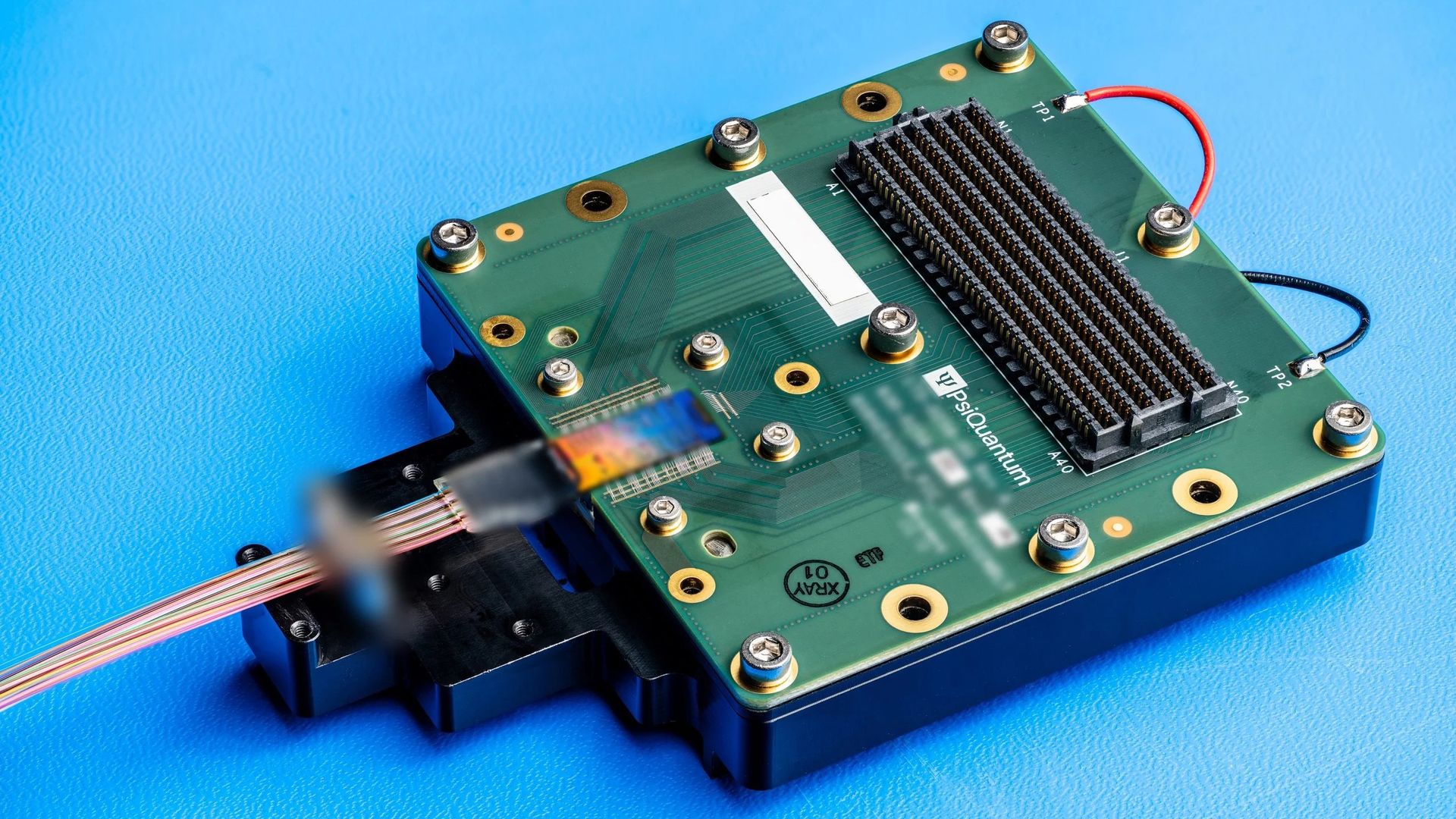
PsiQuantum, a quantum computing company, announced in a release earlier this week that it has turned its low-loss silicon photonics into an optical switch for use in AI data centers. Every optical switch typically comes with loss of light: the more light a switch receives, the less reaches the other side, with the amount of light lost measured in decibels. Typical data center optics can tolerate half the light (3 dB) being lost. PsiQuantum's switch debuted with a demo that typically loses only 1.2 dB of signal, or about a quarter of the light in lab tests, and the all-optical switch can achieve it without an amplifier. The prototype is, however, comparatively small, with eight inputs and outputs (8x8) against competitors’ 32 to 300, but the company says larger devices are in development.

The optical circuit switch (OCS) passes light straight through, from fiber to fiber, without converting it to or from electrical signals. Regular data center switches make that conversion at every hop, which takes power and adds latency. An OCS, instead, uses a fixed light path that it maintains until a change is ordered. Its main penalty comes down to how much light is lost when passing through the switch. PsiQuantum’s switch, which uses circuits etched on a silicon chip with no moving parts, unlike Google’s and Lumentum’s tiny mirrors, or microelectromechanical systems (MEMS), would be used alongside regular packet switches.

Skipping those conversions matters more as AI clusters grow, because moving data between GPUs is quickly becoming a bottleneck. Optics are a high-bandwidth improvement over copper, which has limitations in reach, although a shortage of lasers is a problem for the alternative. Improving communication bandwidth and distance is the goal, so that different racks of GPUs can talk at speed and act as one.

Switches similar to PsiQuantum’s made by Salience Labs and iPronics use built-in amplification and, at least in the former case, are also rated at under 2 dB, or under 37% of the light lost. Google’s mirror-based switch, Palomar, can also typically stay under 2 dB and has 136 ports. Salience’s switch sits at 32 and Lumentum’s at 300, which leaves the eight-port prototype a ways behind on how many fibers it can handle.

Optical circuit switches by loss and size

Switch

Ports (in × out)

Insertion loss, and what the figure is

Reconfiguration

How it switches

PsiQuantum 8×8 demo

8×8

1.2 dB (about 24% of the light lost), typical in the company’s lab tests

Under 3 ms

Silicon photonics chip, no amplification, no moving parts

Google Palomar

136×136

Typically under 2 dB (under 37% lost) across all port pairings; 2 dB worst case

Milliseconds

MEMS mirrors (moving parts)

Lumentum R300

300×300

Close to 1.5 dB (about 29% lost), typical at start of life, Lumentum’s switching GM told Gazettabyte

Not stated

MEMS mirrors (moving parts)

Salience Labs OC-32M

32×32

Under 2 dB (under 37% lost) port to port, a ceiling, after built-in amplification

Under 300 µs

Silicon photonics chip with amplification

iPronics ONE-32

32 (layout not stated)

Not published

Under 300 µs

Silicon photonics chip with optical amplifiers

PsiQuantum's switch is an 8x8, meaning eight in and eight out, and “every input can reach every output.” It’s also “strictly non-blocking,” so a new connection never disturbs ones already in place. In the lab, it measured a typical 1.2 dB insertion loss, 40 dB of crosstalk (about 0.01% of the light leaking to other ports), and under 3 ms of reconfiguration time, all of which exceed “initial targets set for these devices.” The loss figure is measured fiber to fiber, which includes getting light onto and off the chip but not connector losses, PsiQuantum told Tom’s Hardware Premium.

The platform loses very little light at each component, which matters because a quantum computer can tolerate only so much lost light. PsiQuantum’s 2025 Nature paper reports silicon nitride waveguides losing as little as 0.5 dB per meter (about 11% of the light per meter), splitters 0.5 millidecibels, and crossings 1.2 millidecibels, the last two a few hundredths of a percent of the light or less each.

The company also says chip-to-fiber coupling has reached about 60 millidecibels, roughly 1.4% of the light lost, in its best published lab results, although without a full fiber array attached. Those figures set a best case, not a worst case, for a 64-port switch, since light crosses more components as ports are added and the losses add up.

How much loss is acceptable varies with the optics at the end of each link. Coherent, an optics maker, says that using an OCS can add “up to 3 dB additional insertion loss,” but its transceivers are able to work with that. Lumentum told Gazettabyte that 3 dB is good enough to work with off-the-shelf FR4, DR4, and DR8 optical modules using the switch; those are the standard plug-in options used to link GPU servers and switches, at distances of 500 meters to 2 kilometers. PsiQuantum’s 8x8 is built for the O-band, the wavelength range those modules use. PsiQuantum told Semafor that, to be workable, its switch needed insertion loss under 2 to 3 dB.

The 8x8 prototype was designed for conventional data center traffic and comes in well below the 3 dB loss target in a request from Nvidia for proposals, the company says. The port count marks it as a demonstration vehicle, but PsiQuantum has a 64x64 version taped out with a 72x72 underway and is “actively developing larger devices.” With crossings that lose so little light, the scale-up might hold. PsiQuantum declined to share details on future products, though it says the loss, which may be slightly higher, will stay very low.

Speed remains less important than insertion loss for how OCSes are currently used. Google, which has the most deployments, numbering in the “tens of thousands,” uses its switches to resize TPU pods or to route around failed chips, a job its “millisecond-scale” MEMS switches handle. PsiQuantum’s under 3 ms is within that class, but Salience and iPronics claim less than 300 microseconds for their amplified chip switches, which iPronics highlights for mid-workload network rewiring to hide the switch time while chips compute.

There is quite a lot of room for speed to improve, and PsiQuantum already has a material for that, used in an existing 64-port switch for its quantum systems, which need to switch light at gigahertz rates. The material, barium titanate (BTO), changes how it bends light when a voltage is applied, and the company chose it over lithium niobate, a more common selection, because BTO had the strongest effect it could find. This keeps switching elements short and losses low at speeds roughly a million times faster than the demo. BTO is “not required for the demonstration vehicle or initial products,” which use a thermally switched silicon nitride platform, but it is “an additional path to faster, more advanced future products.”

An argument for starting now is that building thousands of such switches for conventional applications would reduce the risk for the packaging, assembly, and supply chain of parts PsiQuantum builds for quantum computing. AI and quantum computing are “complementary technologies,” it says, and this is the chance to put its technology into action. When PsiQuantum hired Rob Soderbery as an executive vice president in July, it said he would advance its silicon photonics platform, “accelerating its application across AI networking and other next-generation computing infrastructure,” hinting at the roadmap. The company’s CHIPS award was finalized in September for “high-performance optical switches,” among other components.

Co-founder Pete Shadbolt praised Google’s alternative MEMS switch but would prefer to have similar-quality switching on a monolithic chip that needs no moving parts. Nvidia has a stake through its venture arm, NVentures, and collaborates with PsiQuantum on “GPU-QPU integration,” that is, graphics and quantum processing units, as well as silicon photonics. Nvidia also joined rival iPronics’ $125 million round in September to develop its second-generation optical switch.

Right now, inside Google, OCSes rewire AI clusters, and research firm Cignal AI expects most deployments to stay there through the end of the decade; outside of Google, OCS is still at “proof-of-concept and early trial.” The firm raised its market estimates earlier this year, though, roughly threefold for 2026 and by more than 40% for 2029. An opening exists for PsiQuantum in GPU networks, which ties into Nvidia’s interest, though adoption there is expected to be limited until then. The company says samples and testing kits have already gone to several computing companies, including GPU vendors and hyperscalers.

PsiQuantum should have commercial products “announced in the coming months,” along with updates on larger devices, while competitor Salience has already demonstrated 64 ports at this year’s European Conference on Optical Communication. Salience’s roadmap already has 128- and 256-port products. Scaling is always an issue, but if PsiQuantum’s figures, which haven’t been independently verified, hold up at 64 ports without amplifiers, then larger monolithic OCSes are on the way.
✇Tomshardware

Intel patent embeds MicroLEDs in chip packaging — technology may enable embedded optical interconnects through TGVs

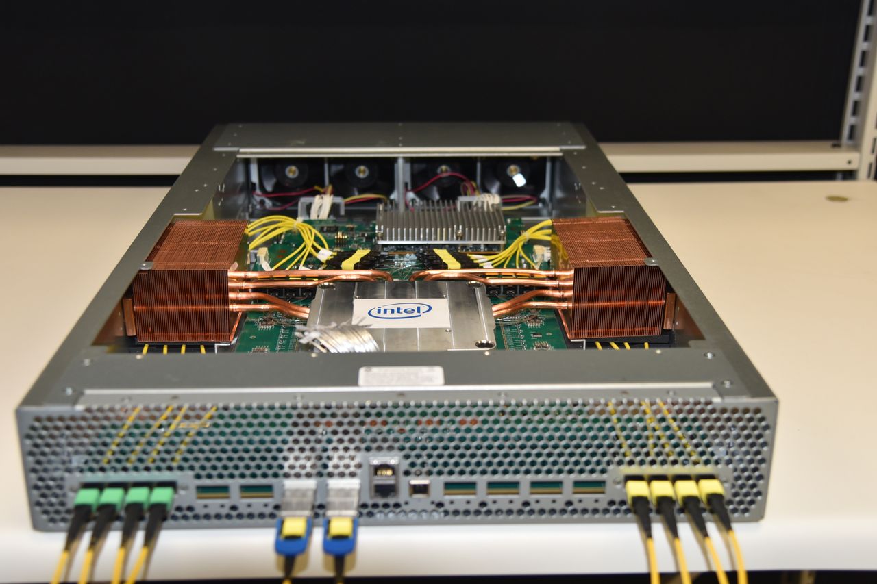
Intel has been granted a U.S. patent that discusses embedding MicroLEDs inside chip packaging, as TrendForce reports. The design embeds semiconductor dies fitted with MicroLEDs directly into a glass substrate and connects them using Through-Glass-Vias (TGV) to provide power and signal connections, allowing them to emit red, green, and blue (RGB) light. Intel suggests this technology could be used for diagnostic testing and to create customized light effects on the chip's surface for personalized electronics and improved aesthetic appeal.

The potential for this to support optical signaling is intriguing, and likely holds significant commercial potential for Intel. Taiwanese optoelectronics firm AU Optronics has a technology roadmap that overlaps with Intel's patent, with some rumored collaboration between the pair, suggesting the two companies may be jointly developing companion technologies in this space.

AUO recently showcased Micro LED optical communication at SEMICON Taiwan 2026, with a design goal interconnect range of up to 10 meters, targeting use in AI data centers. Embedding Micro LEDs into a glass substrate could offer an alternative integration approach for co-packaged optics to Intel's previous demonstration of a co-packaged optical I/O chiplet.

How Intel wants to build chips with glass

In the patent, Intel describes using laser treatment and etching to create the through-holes and die cavities within the glass substrate. It would then use copper electroplating to form the TGVs before embedding the dies carrying MicroLEDs into the substrate. Silicon nitride layers join the glass to polymer package substrates on either side, while conductive vias carry signals and power.

The patent also describes the potential for differing structural variations, including alternative arrangements for horizontal or vertical die placement, and the integration of reflectors to direct light out of the package through the glass substrate.

Intel has been investing in glass substrate technology since the early 2010s and has showcased test packages using glass substrate materials. In January this year, at NEPCON Japan, it demonstrated an engineering sample of a glass core package combined with its EMIB multi-chip module technology.

At ECTC in May, Intel also showcased a 24-layer glass-core panel with copper-filled TGVs, with two embedded EMIB bridges. Arguably more importantly for its chip design and fabrication business, it presented results demonstrating progress towards high-volume manufacturing validation for its glass core substrate designs.

Potential for diagnostics and aesthetics

MicroLEDs built into the chip packaging itself hold potential for diagnostic and testing purposes. They could be used to provide visual indicators of completed tests or failures, without requiring external LEDs or other indicators on motherboards or connected components. Intel's patent doesn't describe a complex diagnostic system, but with pre-determined lighting patterns assigned specific meaning, die-embedded MicroLEDs could provide more streamlined feedback during validation and testing phases.

The patent also discusses the potential for aesthetic use cases of in-package LED lighting. DIY electronics could use it for personalization, including illuminated lettering on the chip's surface. Such designs would need to take cooling into consideration, though. Dies that draw enough power to demand external cooling may not be able to avoid obscuring the MicroLEDs on the package surface.

That could limit this use of the technology to low-power chips, or simply demand a specific heatsink configuration, leaving portions of the packaging bare to ensure the MicroLED light is still visible.

A potentially more significant application of this technology, however, is in an alternative optical interconnect system. The patent doesn't establish a high-speed working optical interconnect, but with AUO's parallel developments in Micro LED CPO modules, the potential is certainly there.

The implications for CPO

MicroLEDs also have potential for optical signaling. AUO's showcase earlier this month highlights this. Combining MicroLED transmitters and Micro photodetector receivers, AUO is developing a system-level MicroLED CPO module designed for high-speed interconnect applications.

Intel's patent could lay the groundwork for something similar. It hasn't proposed that application, nor does the patent make such claims, but embedding MicroLEDs in-package could provide a starting point for integrating optical transmitters.

Embedding emitters is only part of the communication system, though. Where AUO and its partners have showcased MicroLED optical interconnection as a real development direction for CPO, Intel's patent only describes a packaging technique that could support such a system. Like AUO, it would need the receivers and optical fiber solutions to develop a full optical interconnect module.

Intel is clearly investing heavily in glass substrate technologies and has been developing advanced interconnects for years. If it were to partner with AUO on its existing developments, it could accelerate its own efforts in this space and provide an alternative method for bringing interconnects within chip packages.

But that's still very much up in the air. Until Intel makes a more concrete announcement, this is more potential than actual.

✇Tomshardware

Tower Semiconductor to invest $4 billion in Japanese ops to set up massive optical connectivity hub

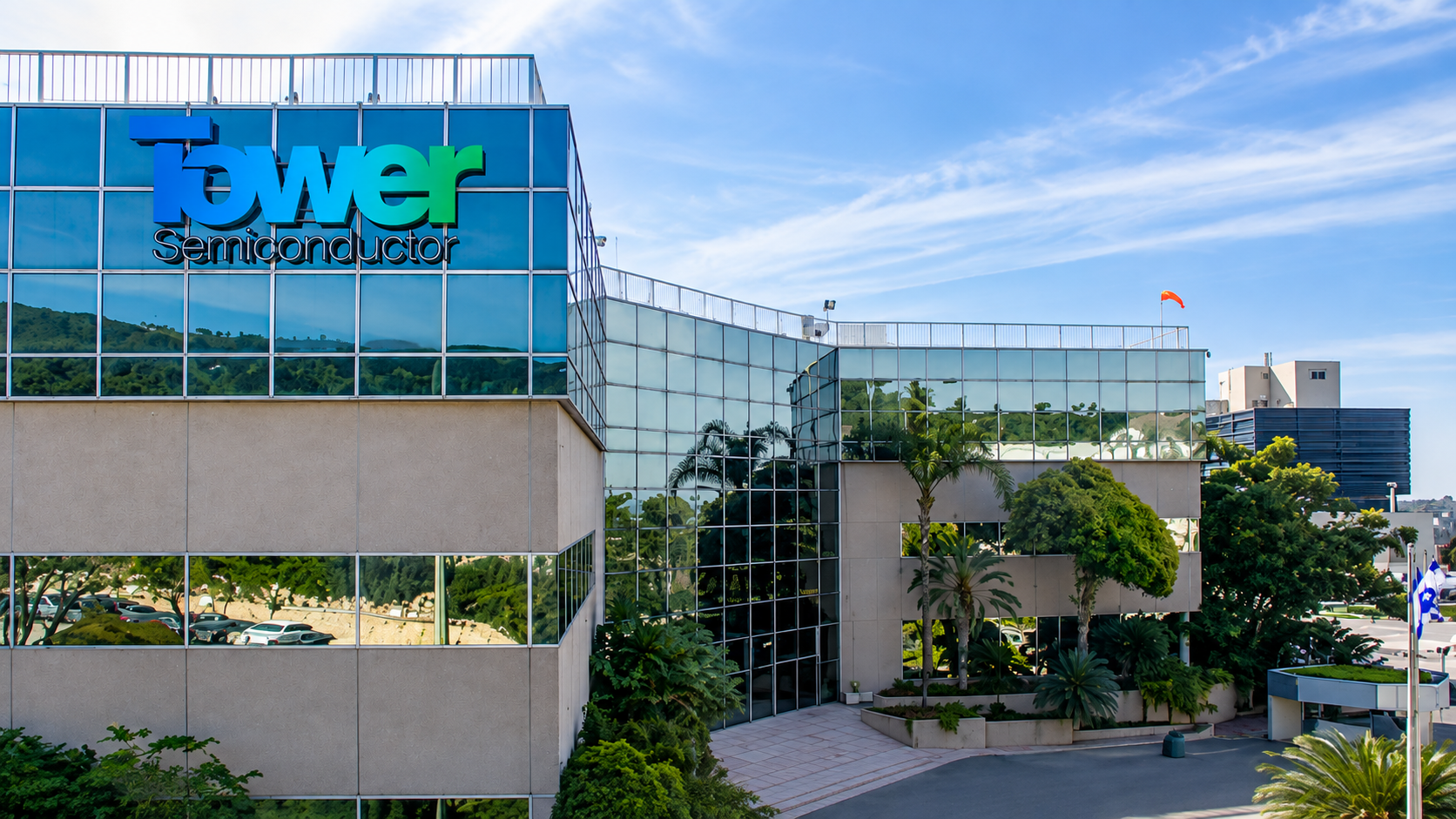
Tower Semiconductor and the government of Japan plan to co-invest a total of $4 billion in the company's Japanese operations to turn regional fabs into a massive manufacturing base for optical-connectivity semiconductors, reports Nikkei. The dual-track expansion will repurpose an idled fab, maximize output of an existing 300mm facility, and eventually add another 300mm fab, thus boosting Tower's Japanese capacity to the equivalent of 45,000 300mm wafers per month by 2029.

Track One: Convert and expand

The first stage, called Track One, involves converting Tower's idle 200-mm Fab 6 in Arai, Niigata Prefecture, into a 300mm manufacturing facility for silicon photonics (SiPho) and advanced optical packaging (i.e., bonding electronic integrated circuits with photonic integrated circuits), as well as expanding the output of SiGe EICs (Silicon-Germanium Electronic Integrated Circuits) and SiPho PICs (Photonic Integrated Circuits) at 300-mm Fab 7 near Uozu, Toyama Prefecture.

Fab 7 is already fully qualified and is in mass production of various SiGe EICs and SiPho PICs using various process technologies, including the latest TPS65SG and several other TPS65-series 65nm-class SiGe fabrication nodes, as well as TPS45PHD 45nm-class SiPho manufacturing technology. The plan is to expand Fab 7's output as significantly as possible to meet growing demand for optical engines by the AI industry. Such an approach enables the company to add output progressively as additional equipment is installed, rather than waiting for an entirely new fab and process flows to qualify.

Track One is scheduled to reach full production readiness in the fourth quarter of 2027. Tower expects Track One to enable it to earn approximately $3.6 billion in revenue and $1.2 billion in net profit in FY2028.

Track Two: Build new fab

The second stage, called Track Two, commences in parallel and is considerably more ambitious. Tower intends to construct another 300mm manufacturing facility next to Fab 7 in Uozu that will increase the company's output of SiGe EICs and SiPho PICs by several times. As a result, Tower will have two sites in Japan producing EICs and PICs and one — the converted Fab 6 — assembling optical engines using these components.

The second stage is expected to start contributing materially to Tower's financial results in 2029.

Tower expects its Japanese production capacity to ultimately reach the equivalent of 45,000 300mm wafers per month in 2029, around 40 times higher than 2025 levels, and plans to hire approximately 200 people. The scale of the project reflects rapidly growing demand for optical connectivity in AI infrastructure. According to Nikkei, Tower controls more than 80% of the contract production market for optical communications semiconductors used in servers and serves some of the industry leaders, including Marvell, so it needs massive scale.

Tower plans to invest $3 billion of its own money in its two expansion tracks, while Japan's Ministry of Economy, Trade and Industry (METI) will provide another $1 billion, bringing the overall project to roughly $4 billion.

Tower admits that companies like Intel, TSMC, and GlobalFoundries are currently ahead in co-packaged optics (CPO), so the Japanese investment is not merely about adding capacity, but also about setting the stage for its CPO plans. For now, Tower intends to bring CPO and preceding manufacturing technologies to its Uozu, Toyama Prefecture, site. While the company has not disclosed any details about its CPO roadmap, even its latest process technologies for EICs and PICs should be more or less good enough to bring optics closer to compute silicon.

Tower's Japan restructuring

Tower Semiconductor's plans for major expansion in Japan also coincide with a restructuring of the company's local manufacturing operations. But understanding what is changing requires a short history lesson.

Tower established its Japanese manufacturing presence in 2014 by forming TowerJazz Panasonic Semiconductor Co. (TPSCo) with Panasonic, owning a 51% controlling stake while Panasonic retained 49% and contributed its fabs in Uozu, Tonami, and Arai. Following Panasonic's exit from the semiconductor business in 2020, Panasonic's stake passed to Nuvoton Technology Corporation Japan (NTCJ).

The most important asset is Fab 7 in Uozu, a 300mm facility that Tower has gradually transformed from a former Panasonic fab into one of its key specialty manufacturing sites that now supports 65nm-class SiGe and 45nm-class SiPho technologies.

Tower and Nuvoton are now effectively dismantling the original TPSCo structure. Under an agreement announced in March 2026 and expected to close in April 2027, Tower will take full ownership and operational control of Fab 7 and its 300mm foundry business, while Nuvoton will take full ownership of TPSCo and Fab 5 in Tonami. At the same time, Tower is resurrecting the former Arai facility, Fab 6, as a 300mm SiPho and advanced optical packaging site and plans to build another 300mm fab adjacent to Fab 7.

In short, what started as a relatively inexpensive way for Tower to obtain Japanese manufacturing capacity from Panasonic more than a decade ago is now evolving into a major Tower-owned 300mm SiPho and SiGe production hub, which is set to increase the company's output and revenue by multiple times.

✇Tomshardware

AI data center optical interconnect market to hit $144 billion by 2030, an over ten-fold increase from 2024 figures, according to new projections — silicon photonics expected to account for nearly two-thirds of revenue, driven by co-packaged optics

The global data center optical interconnect market is expected to reach $144.4 billion by 2030, up from $13.7 billion in 2024 — a 48.1% compound annual growth rate (CAGR) — according to a China Insights Consultancy (CIC) report commissioned by a Chinese laser-chip maker, Yuanjie Semiconductors, as part of its Hong Kong IPO filing. The report draws on data from LightCounting and interviews with industry experts. Of that future market, silicon photonics, the practice of manufacturing photonic chips from the same silicon material and mature CMOS foundry processes used for conventional semiconductors, is projected to account for 63.7% of revenue, its share climbing from 16.6% in 2020 as the industry shifts toward denser, more power-efficient designs like co-packaged optics.

The moves that would turn those projections into reality are already well underway. Over the past year, the AI industry has invested more than $15 billion in co-packaged optics, photonic chips, higher-speed transceiver modules, and fiber, developing new integration techniques, acquiring photonics startups, and forming alliances among the biggest players. More recently, OpenLight and Tower Semiconductor placed OpenLight's photonic design kit inside Cadence's mainstream chip-design software. This step makes the laser-integrated 400G and 1.6T chips at the heart of co-packaged optics easier to design and bring to market.

The tech behind the numbers

For decades, data centers have relied largely on copper traces and cables to move data across circuit boards, within racks, and across clusters. Copper is cheap, reliable, and easy to integrate. However, its power consumption and signal losses increase sharply with bandwidth and distance. As AI data centers are packed with ever more powerful GPUs, shuttling enormous volumes of data and pushing networks toward higher speeds, copper hit a wall. Past a few hundred gigabits per lane, its usable reach collapses to a meter, or two, before signal loss and power draw become unmanageable.

The solution has been a transition to photonics, moving data as light instead of electrical signals. An optical transceiver converts electrical signals from switches and processors into laser light, sends it down a fiber, and converts it back at the far end, carrying far more bandwidth over greater distances at much higher speeds. Today, pluggable transceivers pack a laser chip, digital signal processor (DSP) chips, and several optical components into one compact module. As GPUs grow more capable and AI workloads swell, both the volume of data and the speed it must travel keep climbing, pushing the industry from 400G links to 800G to 1.6T and beyond

At the same time, the industry is trying to move the optics closer to the compute. In conventional systems, GPU signals travel inches along copper traces across the board to reach the transceiver on the faceplate. At extreme data rates, even that relatively short electrical journey consumes considerable power. Co-packaged optics (CPO) fixes this by pulling the optical engine out of the pluggable module and placing it as a chip — the photonic integrated circuit (PIC) — directly on the switch or accelerator package, shrinking the electrical path to millimeters. The push for faster optical chips, aiming for terabits-per-second speeds, serves both CPO and the pluggable modules that remain the industry mainstay.

The PIC does everything but generate light. Because laser chips are highly sensitive to heat, they can't be folded into the PIC, which, in co-packaged optics, becomes part of the switch or accelerator package that runs extremely hot. Therefore, the laser stays a separate chip. Whether feeding a co-packaged PIC or a pluggable module, those laser chips are always needed, which is exactly what Yuanjie, the company that commissioned the CIC forecast, makes.

The PIC itself is where silicon photonics comes in. Photonic chips were once built entirely from costly III-V materials in specialized fabs; Silicon Photonics (SiPh) instead patterns the optical circuitry onto silicon using the same mature, high-volume CMOS processes as ordinary chips — saving money and time and making PICs mass-producible. On the other hand, silicon cannot lase. As a result, laser chips still rely on the more expensive III-V method, using materials such as indium phosphide. Circumventing exactly that is the aim of the recent OpenLight–Tower platform. Their approach integrates III-V laser material directly with silicon photonics at the wafer level, aiming to bring the laser into the same scalable manufacturing flow as the rest of the PIC.

The numbers behind the growth

Together, the different photonics technologies solving the AI data transfer bottleneck are driving a huge market in the industry. CIC projects the data center optical interconnect market growing from $13.7 billion in 2024 to $144.4 billion in 2030, a compound annual growth rate of 48.1%, more than a tenfold increase in six years. Growth accelerates over this period, with the steepest gains occurring after 2027. The report breaks down the three main ways: technology, use case, and data rates, each showing where the spending and resulting revenue are concentrated.

By technology, it splits the market between silicon photonics and everything else. SiPho's share climbs from 16.6% in 2020 to 63.7% of total revenue ($91.9 billion) by 2030, with its revenue compounding at 68.5% annually, compared with 32.6% for the rest, and the crossover past half the market landing around 2027. According to CIC, silicon-based optics— primarily PICs — will grow to become the default.

The use-case breakdown shows which parts of data center networking are driving optical demand: scale-up inside the rack, scale-out across a data center, and scale-across between data centers. Scale-up — the short-reach links from servers and chips to the top-of-rack switch — takes the lead with a 561.5% CAGR in revenue. Note that this figure compounds off a near-zero 2024 base, where a tiny absolute gain reads as an absurd percentage. Scale-across follows at 108.5% and scale-out at 42.7%, while the entire non-AI segment, traditional workloads from telecom to enterprise servers, trails at 37.5%. However, in actual revenue and not growth, scale-out is the largest tier at $64.5 billion in 2030, followed by non-AI at $40.2 billion and scale-up, for all its headline growth — at just $32.1 billion, with scale-across last at $7.6 billion.

The data-rate breakdown captures a generational migration of speed. In 2024, the market still ran on the previous two generations, 400G at $5.9 billion and 800G at $4.5 billion, with legacy 200G-and-below links adding another $3.3 billion and the faster tiers barely registering. By 2030, that order is inverted. 1.6T, only entering commercial deployment in 2026, becomes the single biggest segment at $65.6 billion, expanding at an 867.3% CAGR from a 2024 base of essentially zero; 3.2T, a category that didn't exist in 2024 at all, appears only from 2027 and still vaults to $44.5 billion. Together, those two next-generation speeds make up roughly $110 billion of the $144.4 billion total. The rest slides down the ladder: 800G stays healthy at a 34.8% CAGR to $26.7 billion, but 400G flatlines — 1.0% annual growth to $6.3 billion, after leading the prior cycle at 75.3% — and 200 G and below actively contracts, shrinking 15.4% a year.

The moves behind the numbers

While the CIC figures are just projections, the actual moves happening in the industry point in the same direction. Over roughly the past year, more than $15 billion has moved through silicon photonics. Nvidia invested $2 billion each into Coherent and Lumentum — makers of the lasers and optical components that go inside transceivers — in March, followed by $2 billion into Marvell and a $500 million warrant deal with fiber maker Corning, each bundled with multi-year purchase commitments. Meanwhile, Microsoft, Meta, and OpenAI have teamed up with hardware giants Broadcom, AMD, and Nvidia to establish an Optical Compute Interconnect (OCI) Multi-Source Agreement (MSA) group to develop protocol-agnostic scale-up interconnection technology for AI clusters.

On the mergers-and-acquisitions side, Marvell, before the Nvidia investment, closed its $3.25 billion cash-and-stock acquisition of Celestial AI, a photonic interconnect startup, to gain its Photonic Fabric platform for linking chips optically inside the rack. Meanwhile, Ayar Labs, which builds optical I/O chiplets that move data directly off the compute package, raised a $500 million round at a valuation of roughly $3.75 billion. Elon Musk also received regulatory approval to acquire Mesh, an optical transceiver manufacturer.

Those bets converge on co-packaged optics as the architectural prize. Nvidia's Spectrum-X and Quantum-X photonics switches, built on TSMC's COUPE process, are the flagship deployments. Broadcom is pushing its own CPO Tomahawk line and has foundries TSMC and GlobalFoundries, with Tower supplying the silicon underneath. The one constraint the money cannot instantly buy away is the laser: high-speed III-V sources remain the scarce link, with Lumentum currently the only vendor shipping the 200G-per-lane EMLs that 1.6T modules require at volume. That scarcity — and the whole industry's dependence on laser chips regardless of which design wins — is exactly why a supplier like Yuanjie sits aligned with wherever the market goes.

✇Tomshardware

How optical interconnects and silicon photonics emerged as AI's next hot commodity — looming US-China summit puts photonics into the crosshairs

The race to solve AI's copper bottleneck for scale-up and scale-out intensified last week, as the Federal Communications Commission (FCC) is drafting a measure that would block imports of new Chinese transceiver models, with officials hoping to publish the rule before the end of 2026. Yesterday, we covered exactly how much of the Secure Networks Act might rely on Chinese-made optical module manufacturers.

The technology is currently driving billions in acquisitions among companies like Marvell and Nvidia, and sending stock prices for dedicated Western Photonics companies like Coherent and Lumentum skyrocketing, amid calls that key materials like indium phosphide are in short supply.

Following the FCC's Secure Networks Act proposal, the market reacted immediately, with shares of China’s Zhongji Innolight, Eoptolink, and TFC Optical tumbling in early Shenzhen trading. Meanwhile, U.S. rivals Coherent and Lumentum closed 12.4% and 8.9% higher. Before Wednesday ended, however, the Chinese companies had clawed back much of the ground, even as analysts downplayed the impact of such a ban. Innolight still finished 7.3% lower in Shenzhen, while TFC actually closed 2.3% higher.

The whipsawing market movement was an apt representation of the potential implications of such a ban. Photonics, the industry's answer to its latest bottleneck of moving data between chips, is arguably the hottest technology in AI infrastructure right now. It is also a market defined by deep mutual entanglement. However, the FCC's proposal conveniently overlooks the fact that the biggest customer of China's photonics hardware is the United States.

With a crucial U.S.-China summit looming in September, the AI supply chain is being weaponized, once again, for global trade and supply negotiations, turning Silicon Photonics into a bargaining chip.

AI's latest bottleneck is now a US-China tech wars battleground

As AI clusters scale into the hundreds of thousands of processors, the biggest problem is moving data between them. Computing tasks on frontier AI models are distributed across thousands of GPUs using parallel computing techniques. This setup requires the processors to exchange huge volumes of data multiple times a second. Copper interconnects still dominate, but as per-lane signaling climbs toward 200 Gbps, attenuation and crosstalk make passive copper impractical beyond a meter or two. Optical transceivers solve that problem by converting a chip's electrical signals into photons for transmission over fiber and back again, carrying far more data over longer distances at lower power.

As we examined in our recent detailed AI photonics roadmap, Vendors are racing from 800G modules to 1.6T parts while shortening electrical paths with co-packaged optics, which moves optical engines even closer to switch ASICs and, eventually, accelerators. The race to solve AI's photonics bottleneck is therefore becoming as strategically important as securing GPUs and HBM.

The money is already moving accordingly. Nvidia has reportedly committed $4 billion across Coherent and Lumentum to lock up supply. Elsewhere, Marvell agreed to pay $3.25 billion upfront for silicon photonics startup Celestial AI, with earnouts potentially taking the deal to $5.5 billion. At the same time, Elon Musk has received FTC clearance to acquire Mesh Optical. Meanwhile, Microsoft, Meta, and OpenAI have teamed with Broadcom, AMD, and Nvidia in an optical interconnect alliance to develop an open optical scale-up interconnect.

China has been building its own stack. Wuxi's CHIPX pilot line — the country's first dedicated photonic chip fab — began mass-producing six-inch photonic wafers in 2025. Shanghai opened a state photonic computing laboratory in June alongside newly listed startup Lightelligence. Crucially, Chinese officials note photonic chips don't require the EUV lithography tools Washington has cut off.

Commercially, China appears to be currently leading the market. Chinese vendors account for nearly two-thirds of global transceiver unit shipments and roughly 60% of datacom transceiver revenue, according to Counterpoint Research. Innolight — fresh off a $6.8 billion Hong Kong IPO, the city's biggest this year — leads with a 27% revenue share, ahead of Coherent's 17%, with Eoptolink third and Lumentum at roughly 6%.

However, those figures do not reveal the deep-seated supply-chain entanglements that severely complicate any ban. Innolight and Eoptolink reportedly supply the majority of 800G modules in Nvidia's AI clusters, while pairing DSP chips from Broadcom and Marvell with laser components from Lumentum, Coherent, and Mitsubishi Electric. Western rivals, in turn, need Chinese indium phosphide — export-controlled by Beijing since 2025 — for their lasers.

The U.S. ban

It is amid the intense photonic race, marked by co-dependency between the two countries, that the FCC is seeking to ban related Chinese hardware. Reuters says the agency is drafting a rule that would deny new models of Chinese optical transceivers the equipment authorization they need to be imported, marketed, or sold in the US.

Washington fears the transceivers could become vectors for data theft, malware, or service disruption, with officials reportedly seeking to avoid another Huawei situation, in which Chinese telecom hardware became so embedded in U.S. infrastructure that removing it proved slow and expensive.

If enacted, the rule would be the latest round in a years-long technology conflict spanning security fears and market dominance, one that has extended squarely into AI. On the inbound side, the FCC has banned Huawei gear since 2019. It added foreign-made drones to its Covered List in December 2025, new consumer routers in March, and power inverters and advanced robots in July — each time citing national security. On the outbound side, Washington restricts AI GPUs, ASML's EUV machines, chipmaking tools, and manufacturing tech from reaching China, aiming to slow its AI ascent.

The Trump administration has argued that these bans have barely had any impact on the U.S. economy while enhancing national security. A photonics ban may be more consequential. The U.S. is effectively contemplating short-term disruption to prevent a scenario where the next generation of a critical AI technology, the optical layer of every future data center, would be Chinese hardware. On the other hand, the FCC appears to accept the current supply chain reliance, as the millions of Chinese modules already installed would stay put.

China’s response

For every ban the US issues, Beijing insists it emerges stronger. Officials credit the chip restrictions with forcing focus. Chinese firms delivered 1.65 million AI GPUs in 2025, with homegrown suppliers like Huawei and Cambricon ramping up production as Nvidia's local market share fell below 60%. Domestic firms are also developing alternative manufacturing approaches. Prinano recently claimed wafer-scale photonic-chip production using nanoimprint lithography instead of DUV, although important yield and volume data remain undisclosed. China now says it doesn't even want American chips, blocking Nvidia H200 imports while certifying domestic accelerators for state procurement.

The photonics response has been similar, this time with open displeasure. China's Foreign Ministry said it "firmly opposes" the potential restriction and accused Washington of overstretching national-security concerns. Chinese legal and market analysts told SCMP that existing approved modules should remain unaffected. They argued that Western suppliers lack the packaging capacity, cleanrooms, and manufacturing scale to replace Chinese production within the next few years.

Dai Menghao of law firm King & Wood, quoted in the SCMP report, called the measure "relatively mild," expecting a framework like the FCC's router and inverter rules, where approved hardware keeps selling, and only new models face denial. That comparison doesn't exactly match. Routers, unlike photonics, are a mature category. In a market right in the middle of a transition, almost everything shipping into next-generation builds would fall under the "new model" category.

Still, Chinese experts insist Washington is underestimating its own exposure. "The market and policymakers tend to underestimate how dependent the AI infrastructure ecosystem remains on Chinese optical-module vendors," said Neil Shah, vice-president of research at Counterpoint. "Replacing that capacity within the next couple of years would be very difficult."

For now, the rule that would affect a ban remains a draft, subject to comment periods, carve-outs, and court challenges. With a potential US-China summit looming in September, the world's most important AI component has now potentially turned into a geopolitical flashpoint.

❌